Datasheet Summary
ICS9370 5
DDR Phase Lock Loop Zero Delay Clock Buffer
Remended Application: DDR Zero Delay Clock Buffer
Product Description/Features
:
- Low skew, low jitter PLL clock driver
- I2C for functional and output control
- Feedback pins for input to output synchronization
- Spread Spectrum tolerant inputs
- 3.3V tolerant CLK_INT input
Switching Characteristics:
- PEAK
- PEAK jitter (66MHz): <120ps
- PEAK
- PEAK jitter (>100MHz): <75ps
- CYCLE
- CYCLE jitter (66MHz):<120ps
- CYCLE
- CYCLE jitter (>100MHz):<65ps
- OUTPUT
- OUTPUT skew: <100ps
- Output Rise and Fall Time: 450ps
- 950ps
- DUTY CYCLE: 49%
- 51%
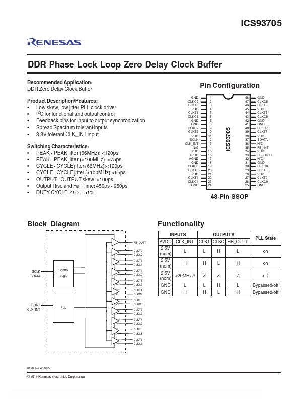
Pin Configuration
GND CLKC0 CLKT0
VDD CLKT1 CLKC1
GND GND CLKC2 CLKT2 VDD SCLK...