ICS859S0212I
ICS859S0212I is Differential-to-LVPECL/LVDS Clock Multiplexer manufactured by Renesas.
Description
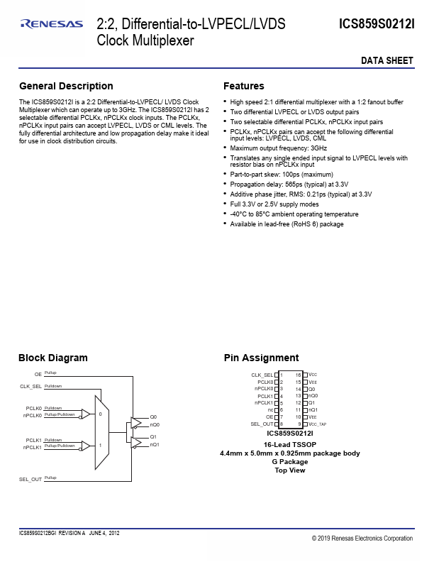
The ICS859S0212I is a 2:2 Differential-to-LVPECL/ LVDS Clock Multiplexer which can operate up to 3GHz. The ICS859S0212I has 2 selectable differential PCLKx, n PCLKx clock inputs. The PCLKx, n PCLKx input pairs can accept LVPECL, LVDS or CML levels. The fully differential architecture and low propagation delay make it ideal for use in clock distribution circuits.
Features
- High speed 2:1 differential multiplexer with a 1:2 fanout buffer
- Two differential LVPECL or LVDS output pairs
- Two selectable differential PCLKx, n PCLKx input pairs
- PCLKx, n PCLKx pairs can accept the following differential input levels: LVPECL, LVDS, CML
- Maximum output frequency: 3GHz
- Translates any single ended input signal to LVPECL levels with resistor bias on n PCLKx input
- Part-to-part skew: 100ps (maximum)
- Propagation delay: 565ps (typical) at 3.3V
- Additive phase jitter, RMS: 0.21ps (typical) at 3.3V
- Full 3.3V or 2.5V supply modes
- -40°C to 85°C ambient operating temperature
- Available in lead-free (Ro HS 6) package
Block Diagram
OE Pullup CLK_SEL Pulldown
PCLK0 Pulldown n PCLK0 Pullup/Pulldown
PCLK1 Pulldown n PCLK1 Pullup/Pulldown
Q0 n Q0
Q1 n Q1
SEL_OUT Pullup
ICS859S0212BGI REVISION A JUNE 4, 2012
Pin Assignment
CLK_SEL 1
16 VCC
PCLK0 2
15 VEE n PCLK0 3 14 Q0
PCLK1 4 13 n Q0 n PCLK1 5 12 Q1 nc 6 11 n Q1
OE 7
10 VEE
SEL_OUT 8
9 VCC_TAP
16-Lead TSSOP 4.4mm x 5.0mm x 0.925mm package body
G Package Top View
©2012 Integrated Device Technology, Inc.
ICS859S0212I Data Sheet
2:2, DIFFERENTIAL-TO-LVPECL/LVDS CLOCK MULTIPLEXER
Table 1. Pin Descriptions
Number...