Datasheet4U Logo Datasheet4U.com
Renesas logo

ICS8305I-02 Datasheet

Manufacturer: Renesas
ICS8305I-02 datasheet preview

Datasheet Details

Part number ICS8305I-02
Datasheet ICS8305I-02-Renesas.pdf
File Size 1.31 MB
Manufacturer Renesas
Description LVCMOS-to-LVCMOS Fanout Buffer
ICS8305I-02 page 2 ICS8305I-02 page 3

ICS8305I-02 Overview

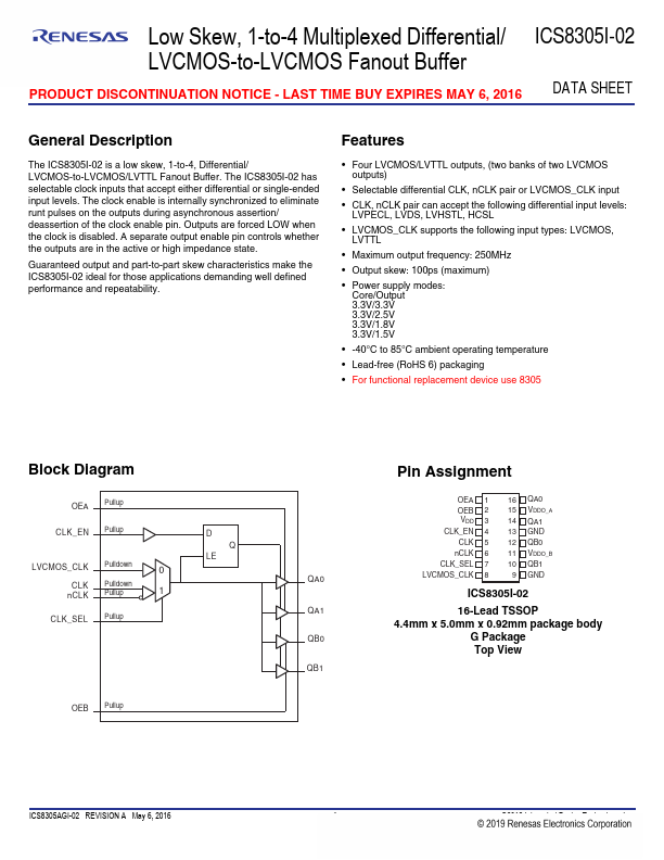
The ICS8305I-02 is a low skew, 1-to-4, Differential/ LVCMOS-to-LVCMOS/LVTTL Fanout Buffer. The ICS8305I-02 has selectable clock inputs that accept either differential or single-ended input levels. The clock enable is internally synchronized to eliminate runt pulses on the outputs during asynchronous assertion/ deassertion of the clock enable pin.

ICS8305I-02 Key Features

  • Four LVCMOS/LVTTL outputs, (two banks of two LVCMOS
  • Selectable differential CLK, nCLK pair or LVCMOS_CLK input
  • CLK, nCLK pair can accept the following differential input levels
  • LVCMOS_CLK supports the following input types: LVCMOS
  • Maximum output frequency: 250MHz
  • Output skew: 100ps (maximum)
  • Power supply modes
  • 40°C to 85°C ambient operating temperature
  • Lead-free (RoHS 6) packaging
  • For functional replacement device use 8305
Renesas logo - Manufacturer

More Datasheets from Renesas

See all Renesas datasheets

Part Number Description
ICS8305I LVCMOS-TO-LVCMOS/LVTTL FANOUT BUFFER
ICS8305 LVCMOS-to-LVCMOS/LVTTL Fanout Buffer
ICS83056I-01 SINGLE-ENDED LVCMOS MULTIPLEXER
ICS831721I Differential Clock/Data Multiplexer
ICS83210 HSTL Fanout Buffer
ICS83940DI LVCMOS/LVTTL Fanout Buffer
ICS840022I-02 Crystal-to-LVCMOS/LVTTL Clock Generator
ICS840051I CRYSTAL-TOLVCMOS/LVTTL CLOCK GENERATOR
ICS840N021I-01 Clock Synthesizer
ICS840N202I Universal Frequency Translator

ICS8305I-02 Distributor

Datasheet4U Logo
Since 2006. D4U Semicon. About Datasheet4U Contact Us Privacy Policy Purchase of parts