HD74LVC245A
Description
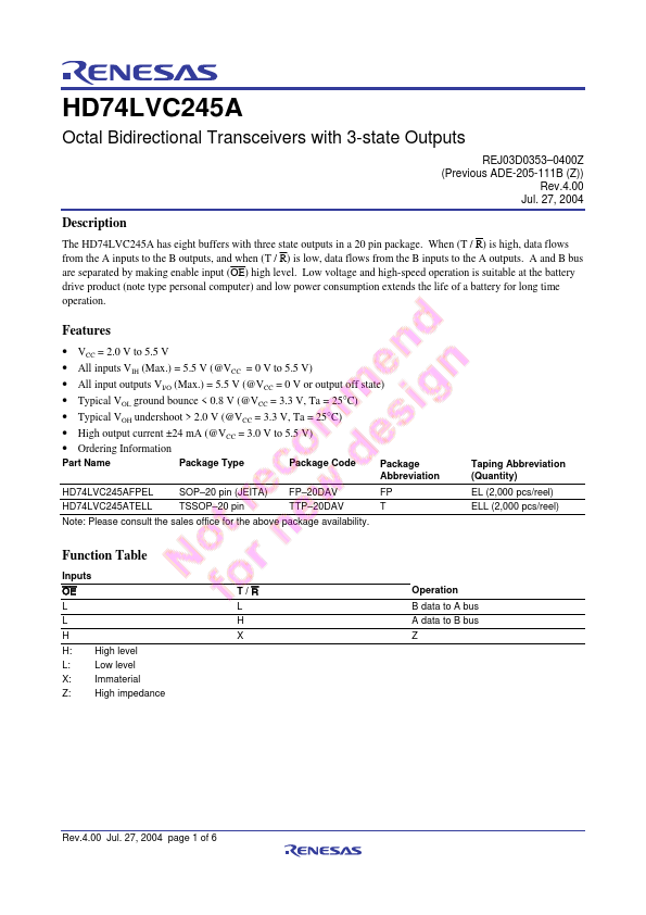
The HD74LVC245A has eight buffers with three state outputs in a 20 pin package. When (T / R) is high, data flows from the A inputs to the B outputs, and when (T / R) is low, data flows from the B inputs to the A outputs.
Key Features
- VCC = 2.0 V to 5.5 V
- All inputs VIH (Max.) = 5.5 V (@VCC = 0 V to 5.5 V)
- All input outputs VI/O (Max.) = 5.5 V (@VCC = 0 V or output off state)
- Typical VOL ground bounce < 0.8 V (@VCC = 3.3 V, Ta = 25°C)
- Typical VOH undershoot > 2.0 V (@VCC = 3.3 V, Ta = 25°C)
- High output current ±24 mA (@VCC = 3.0 V to 5.5 V)


