HD74CDCV857A
Overview
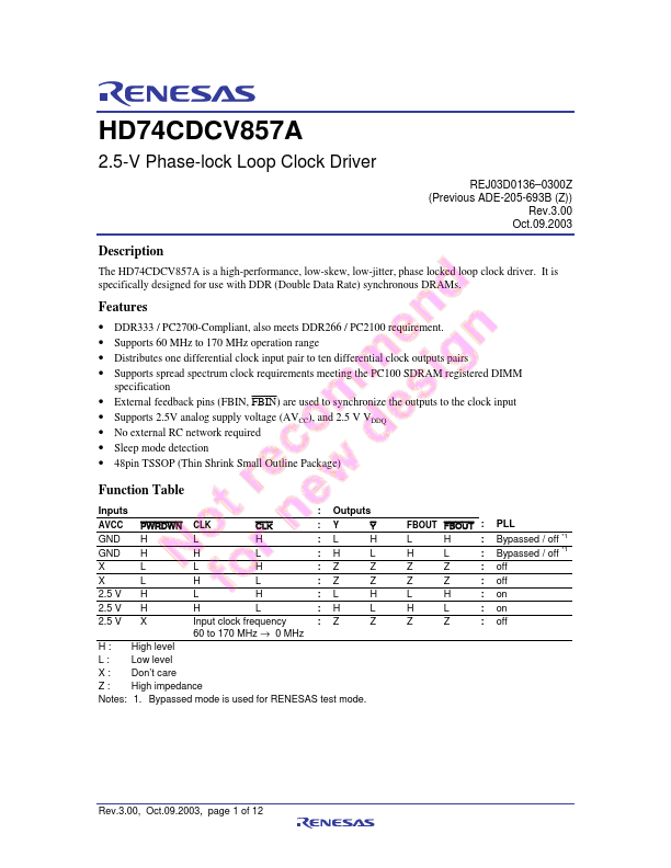
The HD74CDCV857A is a high-performance, low-skew, low-jitter, phase locked loop clock driver. It is specifically designed for use with DDR (Double Data Rate) synchronous DRAMs.
- DDR333 / PC2700-Compliant, also meets DDR266 / PC2100 requirement.
- Supports 60 MHz to 170 MHz operation range
- Distributes one differential clock input pair to ten differential clock outputs pairs
- Supports spread spectrum clock requirements meeting the PC100 SDRAM registered DIMM