Datasheet4U Logo Datasheet4U.com

EL7155 - High Performance Pin Driver

General Description

PIN PIN # NAME FUNCTION 1 VS+ Positive Supply Voltage 2 OE Output Enable EQUIVALENT CIRCUIT VS+ INPUT VL Circuit 1 3 IN Input Reference Circuit 1 4 GND Ground 5 VL Negative Supply and Lower Output Voltage 6 OUTL Lower Switch Output VS+ OUTL Ordering Information PART NUMBER (Notes 1,

Key Features

  • Clocking speeds up to 40MHz.
  • 15ns tr/tf at 2000pF CLOAD.
  • 0.5ns rise and fall times mismatch.
  • 0.5ns tON-tOFF prop delay mismatch.
  • 3.5pF typical input capacitance.
  • 3.5A peak drive.
  • Low ON-resistance of 3.5Ω.
  • High capacitive drive capability.
  • Operates from 4.5V up to 16.5V.
  • Pb-free (RoHS compliant).

📥 Download Datasheet

Datasheet Details

Part number EL7155
Manufacturer Renesas
File Size 511.66 KB
Description High Performance Pin Driver
Datasheet download datasheet EL7155 Datasheet

Full PDF Text Transcription (Reference)

The following content is an automatically extracted verbatim text from the original manufacturer datasheet and is provided for reference purposes only.

View original datasheet text
EL7155 High Performance Pin Driver 
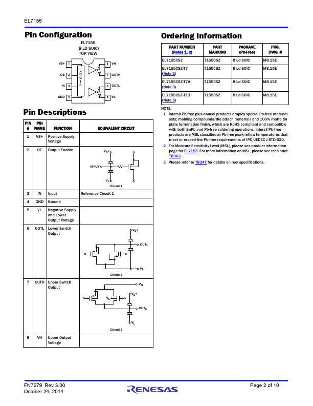
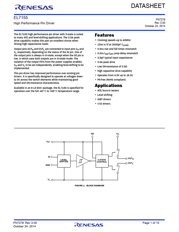
The EL7155 high performance pin driver with 3-state is suited to many ATE and level-shifting applications. The 3.5A peak drive capability makes this part an excellent choice when driving high capacitance loads. Output pins OUTH and OUTL are connected to input pins VH and VL respectively, depending on the status of the IN pin. One of the output pins is always in tri-state, except when the OE pin is low, in which case both outputs are in tri-state mode. The isolation of the output FETs from the power supplies enables VH and VL to be set independently, enabling level-shifting to be implemented. This pin driver has improved performance over existing pin drivers.