Datasheet4U.com
🌙
9DB202 Datasheet | Renesas
Part:
9DB202
Description:
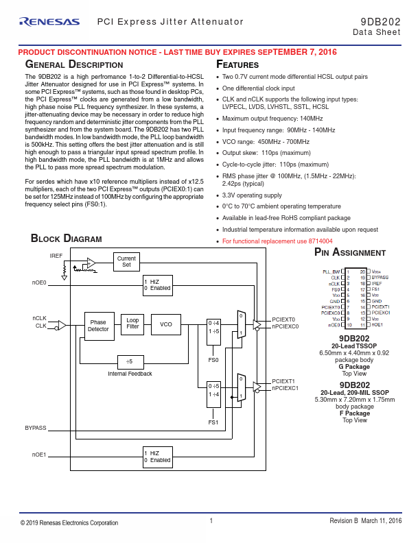
PCI Express Jitter Attenuator
Manufacturer:
Renesas
Size:
328.34 KB
9DB202 Datasheet (PDF) Download
Renesas
9DB202
Overview
Two 0.7V current mode differential HCSL output pairs
One differential clock input
CLK and nCLK supports the following input types:
×
Close