9DB1233 Overview
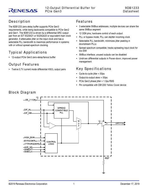
The 9DB1233 zero-delay buffer supports PCIe Gen3 requirements, while being backwards patible to PCIe Gen2 and Gen1. The 9DB1233 is driven by a differential SRC output pair from an IDT 932S421 or 932SQ420 or equivalent main clock generator. It attenuates jitter on the input clock and has a selectable PLL bandwidth to maximize performance in systems with or without spread-spectrum clocking.
9DB1233 Key Features
- Twelve 0.7V current mode differential HSCL output pairs
- 3 selectable SMBus addresses; multiple devices can share the same SMBus segment
- 12 OE# pins; hardware control of each output
- PLL or bypass mode; PLL can dejitter ining clock
- SMBus interface; unused outputs can be disabled
- Undriven differential outputs in Power-down; improved power
- Cycle-to-cycle jitter < 50ps
- Output-to-output skew < 50ps
- PCIe Gen3 phase jitter < 1.0ps RMS
- Pin patible with DB1200 Yellow Cover device