8S89296
Overview
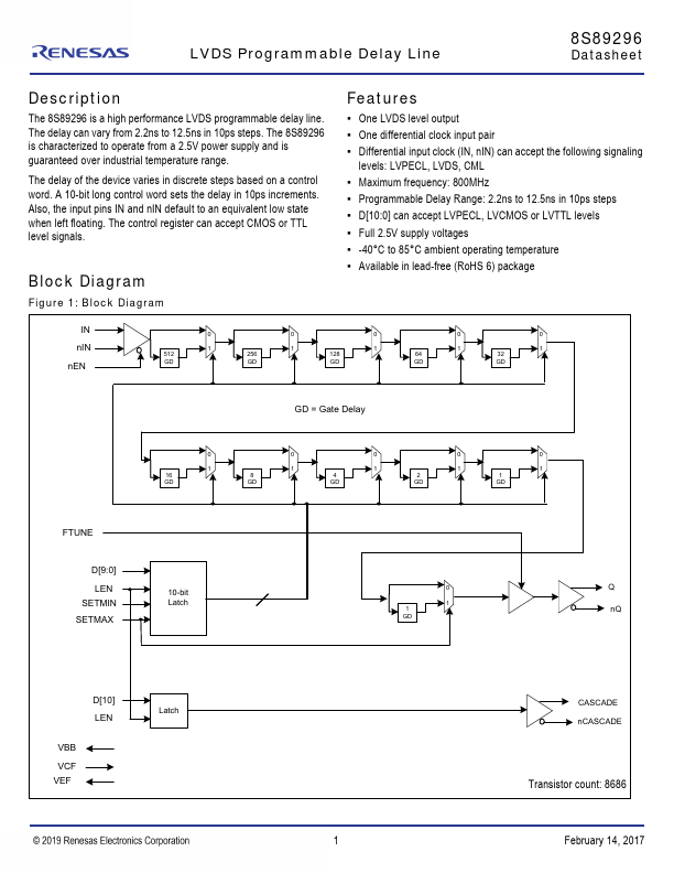
The 8S89296 is a high performance LVDS programmable delay line. The delay can vary from 2.2ns to 12.5ns in 10ps steps.
| Part | 8S89296 |
|---|---|
| Description | LVDS Programmable Delay Line |
| Manufacturer | Renesas |
| Size | 544.20 KB |
The 8S89296 is a high performance LVDS programmable delay line. The delay can vary from 2.2ns to 12.5ns in 10ps steps.
| Part Number | Manufacturer | Description |
|---|---|---|
| DK124 | Dongke Semiconductor | OFF-LINE SWITCH MODE POWER CONTROLLER |
| KP3114 | Kiwi Instruments | High Performance Low Cost Off-line PWM Power Switch |
| KP311AWPA | Kiwi Instruments | High Performance Low Cost Off-line PWM Power Switch |