Datasheet4U Logo Datasheet4U.com
Renesas logo

894D115I-04 Datasheet

Manufacturer: Renesas
894D115I-04 datasheet preview

Datasheet Details

Part number 894D115I-04
Datasheet 894D115I-04-Renesas.pdf
File Size 402.23 KB
Manufacturer Renesas
Description Clock/Data Recovery
894D115I-04 page 2 894D115I-04 page 3

894D115I-04 Overview

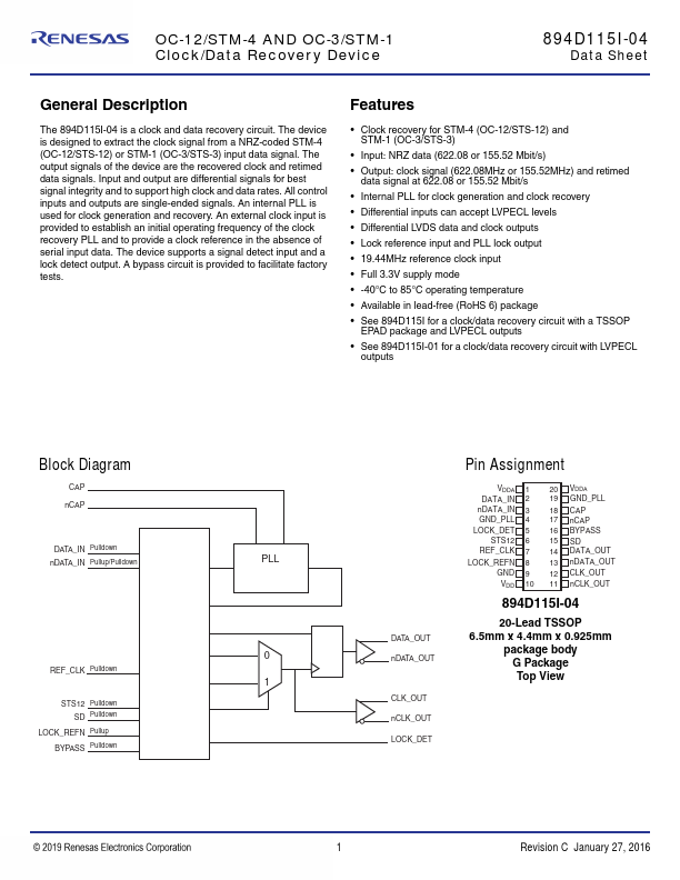
The 894D115I-04 is a clock and data recovery circuit. The device is designed to extract the clock signal from a NRZ-coded STM-4 (OC-12/STS-12) or STM-1 (OC-3/STS-3) input data signal. The output signals of the device are the recovered clock and retimed data signals.

894D115I-04 Key Features

  • Clock recovery for STM-4 (OC-12/STS-12) and
  • Input: NRZ data (622.08 or 155.52 Mbit/s)
  • Output: clock signal (622.08MHz or 155.52MHz) and retimed
  • Internal PLL for clock generation and clock recovery
  • Differential inputs can accept LVPECL levels
  • Differential LVDS data and clock outputs
  • Lock reference input and PLL lock output
  • 19.44MHz reference clock input
  • Full 3.3V supply mode
  • 40°C to 85°C operating temperature
Renesas logo - Manufacturer

More Datasheets from Renesas

See all Renesas datasheets

Part Number Description
894D115I-01 Clock/Data Recovery

894D115I-04 Distributor

Datasheet4U Logo
Since 2006. D4U Semicon. About Datasheet4U Contact Us Privacy Policy Purchase of parts