873996
Overview
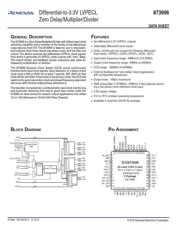
The 873996 is a Zero Delay/Multiplier/Divider with hitless input clock switching capability and a member of the family of low jitter/phase noise devices from IDT. The 873996 is ideal for use in redundant, fault tolerant clock trees where low phase noise and low jitter are critical.
- Six differential 3.3V LVPECL outputs
- Selectable differential clock inputs
- CLKx, nCLKx pair can accept the following differential input levels: LVPECL, LVDS, LVHSTL, HCSL, SSTL
- Input clock frequency range: 49MHz to 213.33MHz
- Output clock frequency range: 49MHz to 640MHz
- VCO range: 490MHz to 640MHz
- External feedback for “zero delay” clock regeneration with configurable frequencies
- Output skew: 100ps (maximum)
- RMS phase jitter (1.875MHz - 20MHz): 0.6ps (typical) assum- ing a low phase noise reference clock input
- 3.3V supply voltage