Datasheet Details
| Part number | 831752 |
|---|---|
| Manufacturer | Renesas |
| File Size | 647.44 KB |
| Description | Clock Switch |
| Datasheet |
 831752 Datasheet 831752 Datasheet
|
|
|
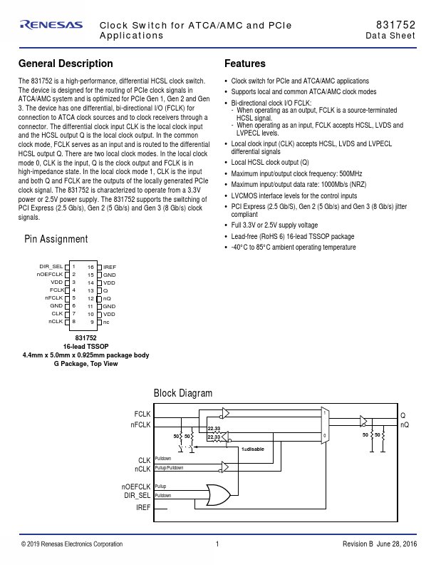
The 831752 is a high-performance, differential HCSL clock switch.
The device is designed for the routing of PCIe clock signals in ATCA/AMC system and is optimized for PCIe Gen 1, Gen 2 and Gen 3.
| Part number | 831752 |
|---|---|
| Manufacturer | Renesas |
| File Size | 647.44 KB |
| Description | Clock Switch |
| Datasheet |
831752 Datasheet
|
|
|
|
| Part Number | Description | Manufacturer |
|---|---|---|
| 831752 | Clock Switch | IDT |
| 831724 | Differential Clock/Data Multiplexer | IDT |
| 831742I | 4:2 Differential Clock/Data Multiplexer | IDT |
| 8310 | Connector Modules with Intergrated LAN Magnetics | ETC |
| 8311 | Connector Modules with Intergrated LAN Magnetics | ETC |
| Part Number | Description |
|---|---|
| 831742I | Differential Clock/Data Multiplexer |
| 83115 | 1-TO-16 LVCMOS/LVTTL Fanout Buffer |
The following content is an automatically extracted verbatim text from the original manufacturer datasheet and is provided for reference purposes only.