Datasheet Details
| Part number | 83115 |
|---|---|
| Manufacturer | Renesas |
| File Size | 321.39 KB |
| Description | 1-TO-16 LVCMOS/LVTTL Fanout Buffer |
| Datasheet | 83115-Renesas.pdf |
|
|
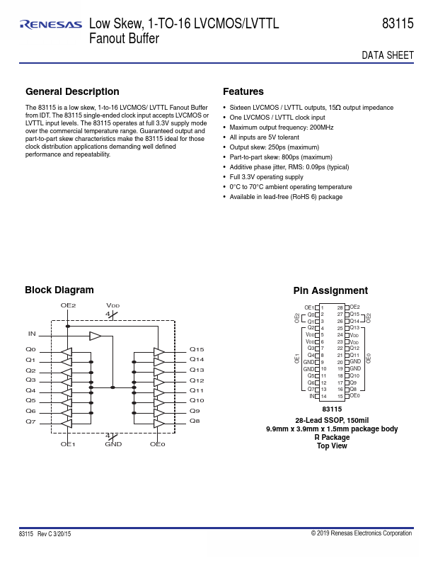
Overview: Low Skew, 1-TO-16 LVCMOS/LVTTL Fanout Buffer 83115 DATA SHEET.
| Part number | 83115 |
|---|---|
| Manufacturer | Renesas |
| File Size | 321.39 KB |
| Description | 1-TO-16 LVCMOS/LVTTL Fanout Buffer |
| Datasheet | 83115-Renesas.pdf |
|
|
|
The 83115 is a low skew, 1-to-16 LVCMOS/ LVTTL Fanout Buffer from IDT.
The 83115 single-ended clock input accepts LVCMOS or LVTTL input levels.
The 83115 operates at full 3.3V supply mode over the mercial temperature range.
| Part Number | Description |
|---|---|
| 831742I | Differential Clock/Data Multiplexer |
| 831752 | Clock Switch |