83026I-01
83026I-01 is 1-to-2 Differential-to-LVCMOS/LVTTL Fanout Buffer manufactured by Renesas.
DESCRIPTION
The 83026I-01 is a low skew, 1-to-2 Differential-to-LVCMOS/LVTTL Fanout Buffer. The differential input can accept most differential signal types (LVPECL, LVDS, LVHSTL, HCSL and SSTL) and translate to two single-ended LVCMOS/LVTTL outputs. The small 8-lead SOIC footprint makes this device ideal for use in applications with limited board space.
FEATURES
- Two LVCMOS / LVTTL outputs
- Differential CLK, n CLK input pair
- CLK, n CLK pair can accept the following differential input levels: LVPECL, LVDS, LVHSTL, HCSL, SSTL
- Maximum output frequency: 350MHz
- Output skew: 15ps (maximum)
- Part-to-part skew: 600ps (maximum)
- Additive phase jitter, RMS: 0.03ps (typical)
- Small 8 lead SOIC package saves board space
- 3.3V core, 3.3V, 2.5V or 1.8V output operating supply
- -40°C to 85°C ambient operating temperature
- Available in lead-free Ro HS (6) package
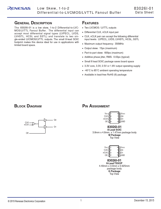
BLOCK DIAGRAM
Q0 CLK n CLK
Q1
PIN ASSIGNMENT
VDD 1 CLK 2 n CLK 3 OE 4
8 VDDO 7 Q0 6 Q1 5 GND
8-Lead SOIC 3.8mm x 4.8mm, x 1.47mm package body
M Package Top View
VDD 1 CLK 2 n CLK 3 OE 4
8 VDDO 7 Q0 6 Q1 5 GND
8-Lead TSSOP 4.40mm x 3.0mm x 0.925mm package body G Package Top View
©2015 Integrated Device Technology, Inc
December 15, 2015
83026I-01 Data Sheet
TABLE 1. PIN DESCRIPTIONS
Number Name
Type
Description
Power
Positive supply pin.
Input Pulldown Non-inverting differential clock input.
3 n...