• Part: 5P49V5933
  • Description: Programmable Clock Generator
  • Manufacturer: Renesas
  • Size: 567.75 KB
Download 5P49V5933 Datasheet PDF
Renesas
5P49V5933
5P49V5933 is Programmable Clock Generator manufactured by Renesas.
Description 
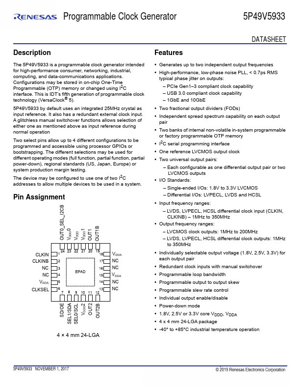
The 5P49V5933 is a programmable clock generator intended for high-performance consumer, networking, industrial, puting, and data-munications applications. Configurations may be stored in on-chip One-Time Programmable (OTP) memory or changed using I2C interface. This is IDT’s fifth generation of programmable clock technology (Versa Clock® 5). 5P49V5933 by default uses an integrated 25MHz crystal as input reference. It also has a redundant external clock input. A glitchless manual switchover functions allows selection of either one as mentioned above as input reference during normal operation Two select pins allow up to 4 different configurations to be programmed and accessible using processor GPIOs or bootstrapping. The different selections may be used for different operating modes (full function, partial function, partial power-down), regional standards (US, Japan, Europe) or system production margin testing. The device may be configured to use one of two I2C addresses to allow multiple devices to be used in a system. Pin Assignment OUT0_SEL_I2CB VDDO0 VDDD VDDO1 OUT1 OUT1B CLKIN CLKINB NC NC VDDA CLKSEL 1 24 23 22 21 20 1918 2 17 3 16 EPAD 4 15 5 14 6 13 7 8 9 10 11 12 VDDA NC NC VDDA NC NC SD/OE SEL1/SDA SEL0/SCL VDDO2 OUT2 OUT2B 4 × 4 mm 24-LGA Features - Generates up to two independent output frequencies - High-performance, low-phase noise PLL, < 0.7ps RMS typical phase jitter on outputs: - PCIe Gen1- 3 pliant clock capability - USB 3.0 pliant clock capability - 1Gb E and 10Gb E - Two fractional output dividers (FODs) - Independent spread spectrum capability on each output pair - Two banks of internal non-volatile in-system programmable or factory programmable OTP memory - I2C serial programming interface - One reference LVCMOS output clock - Two universal output pairs: - Each configurable as one differential output pair or two LVCMOS outputs - I/O Standards: - Single-ended I/Os: 1.8V to 3.3V LVCMOS - Differential I/Os: LVPECL, LVDS and HCSL -...