PCS3P623Z09B
PCS3P623Z09B is Timing-Safe Peak EMI reduction IC manufactured by PulseCore Semiconductor.
- Part of the PCS3P623Z05A comparator family.
- Part of the PCS3P623Z05A comparator family.
Features
- -
- Clock distribution with Timing-Safe™ Peak EMI Reduction Input frequency range: 20MHz
- 50MHz Multiple low skew Timing-safe™ Outputs: PCS3P623Z05: 5 Outputs PCS3P623Z09: 9 Outputs
- -
- - External Input-Output Delay Control option Supply Voltage: 3.3V±0.3V mercial and Industrial temperature range Packaging Information: ASM3P623Z05: 8 pin SOIC, and TSSOP ASM3P623Z09:16 pin SOIC, and TSSOP
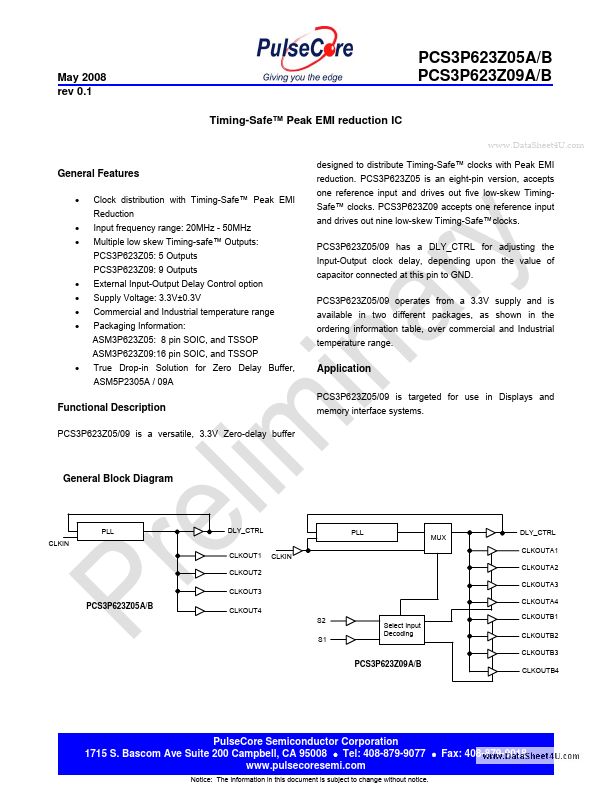
- True Drop-in Solution for Zero Delay Buffer, ASM5P2305A / 09A designed to distribute Timing-Safe™ clocks with Peak EMI reduction. PCS3P623Z05 is an eight-pin version, accepts one reference input and drives out five low-skew Timing Safe™ clocks. PCS3P623Z09 accepts one reference input and drives out nine low-skew Timing-Safe™clocks. PCS3P623Z05/09 has a DLY_CTRL for adjusting the Input-Output clock delay, depending upon the value of capacitor connected at this pin to GND. PCS3P623Z05/09 operates from a 3.3V supply and is available in two different packages, as shown in the ordering information table, over mercial and Industrial temperature range.
Application
PCS3P623Z05/09 is targeted for use in Displays and
Functional Description
PCS3P623Z05/09 is a versatile, 3.3V Zero-delay buffer memory interface systems.
General Block Diagram
PLL CLKIN
DLY_CTRL CLKOUT1 CLKOUT2 CLKOUT3
PLL CLKIN
DLY_CTRL CLKOUTA1 CLKOUTA2 CLKOUTA3 CLKOUTA4
PCS3P623Z05A/B
CLKOUT4 S2 S1 Select Input Decoding
CLKOUTB1 CLKOUTB2 CLKOUTB3
PCS3P623Z09A/B
CLKOUTB4
Pulse Core Semiconductor Corporation 1715 S. Bas Ave Suite 200 Campbell, CA 95008
- Tel: 408-879-9077
- Fax: 408-879-9018 .pulsecoresemi.
Notice: The information in this document is subject to change without notice.
May 2008 rev 0.1
Spread Spectrum Frequency Generation
The clocks in digital systems are typically square waves with a 50% duty cycle and as frequencies increase the edge rates also get faster. Analysis shows that a square wave is posed of fundamental frequency and harmonics. The fundamental frequency and harmonics...