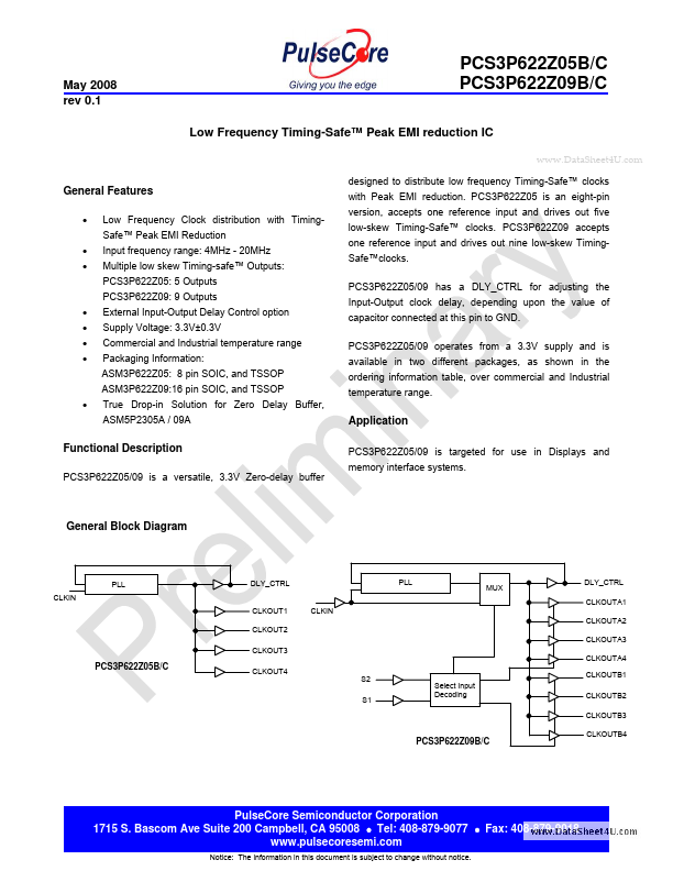
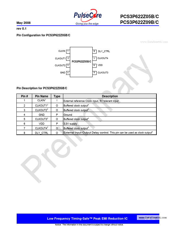
Datasheet4U Logo Datasheet4U.com

PCS3P622Z05B - Low Frequency Timing-Safe Peak EMI reduction IC

Description

PCS3P622Z05/09 is a versatile, 3.3V Zero-delay buffer General Block Diagram PLL CLKIN DLY_CTRL CLKOUT1 CLKOUT2 CLKIN PLL MUX DLY_CTRL CLKOUTA1 CLKOUTA2 CLKOUTA3 CLKOUT3 CLKOUTA4 S2 S1 CLKOUTB1 Select Input Decoding CLKOUTB2 CLKOUTB3 PCS3P622Z05B/C CLKOUT4 PCS3P622Z09B/C CLKOUTB4 PulseCo

Features

  • Low Frequency Clock distribution with TimingSafe™ Peak EMI Reduction Input frequency range: 4MHz - 20MHz Multiple low skew Timing-safe™ Outputs: PCS3P622Z05: 5 Outputs PCS3P622Z09: 9 Outputs.
  • External Input-Output Delay Control option Supply Voltage: 3.3V±0.3V Commercial and Industrial temperature range Packaging Information: ASM3P622Z05: 8 pin SOIC, and TSSOP ASM3P622Z09:16 pin SOIC, and TSSOP.
  • True Drop-in Solution f.

📥 Download Datasheet

Datasheet Details

Part number PCS3P622Z05B
Manufacturer PulseCore Semiconductor
File Size 581.28 KB
Description Low Frequency Timing-Safe Peak EMI reduction IC
Datasheet download datasheet PCS3P622Z05B Datasheet
Other Datasheets by PulseCore Semiconductor

Full PDF Text Transcription

Click to expand full text
May 2008 rev 0.1 PCS3P622Z05B/C PCS3P622Z09B/C Low Frequency Timing-Safe™ Peak EMI reduction IC www.DataSheet4U.com General Features • • • Low Frequency Clock distribution with TimingSafe™ Peak EMI Reduction Input frequency range: 4MHz - 20MHz Multiple low skew Timing-safe™ Outputs: PCS3P622Z05: 5 Outputs PCS3P622Z09: 9 Outputs • • • • External Input-Output Delay Control option Supply Voltage: 3.3V±0.3V Commercial and Industrial temperature range Packaging Information: ASM3P622Z05: 8 pin SOIC, and TSSOP ASM3P622Z09:16 pin SOIC, and TSSOP • True Drop-in Solution for Zero Delay Buffer, ASM5P2305A / 09A designed to distribute low frequency Timing-Safe™ clocks with Peak EMI reduction.
Published: |