CM1200HA-34H
CM1200HA-34H is IGBT Module manufactured by Powerex, Inc.
MITSUBISHI HVIGBT MODULES
HVIGBT (High Voltage Insulated Gate Bipolar Transistor) Modules HIGH POWER SWITCHING USE INSULATED TYPE
CM1200HA-34H q IC 1200A q VCES 1700V q Insulated Type q 1-element in a pack
APPLICATION Inverters, Converters, DC choppers, Induction heating, DC to DC converters.
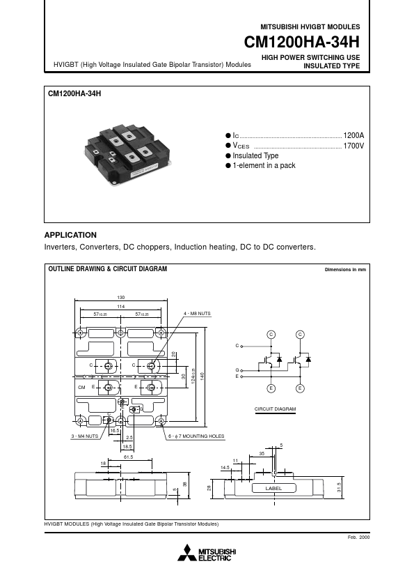
OUTLINE DRAWING & CIRCUIT DIAGRAM
Dimensions in mm
130 114 57±0.25 57±0.25 4
- M8 NUTS
124±0.25 140 30
CIRCUIT DIAGRAM
16.5 3
- M4 NUTS 2.5 18.5 61.5 18
- φ 7 MOUNTING HOLES 5 35 11 14.5
LABEL
HVIGBT MODULES (High Voltage Insulated Gate Bipolar Transistor Modules)
Feb. 2000
MITSUBISHI HVIGBT MODULES
HVIGBT (High Voltage Insulated Gate Bipolar Transistor) Modules HIGH POWER SWITCHING USE INSULATED TYPE
MAXIMUM RATINGS (Tj = 25 °C)
Symbol VCES VGES IC ICM IE (Note 2) IEM (Note 2) PC (Note 3) Tj Tstg Viso
- - Item Collector-emitter voltage Gate-emitter voltage Collector current Emitter current Maximum collector dissipation Junction temperature Storage temperature Isolation voltage Mounting torque Mass VGE = 0V VCE = 0V TC = 25°C Pulse TC = 25°C Pulse TC = 25°C, IGBT part Conditions Ratings 1700 ± 20 1200 2400 1200 2400 12500
- 40 ~ +150
- 40 ~ +125 4000 6.67 ~ 13.00 2.84 ~ 6.00 0.88 ~ 2.00 1.5 Unit V V A A A A W °C °C V N- m N- m N- m kg
(Note 1) (Note 1)
- - Charged part to base plate, rms, sinusoidal, AC 60Hz 1min. Main terminals screw M8 Mounting screw M6 Auxiliary terminals screw M4 Typical value
ELECTRICAL CHARACTERISTICS (Tj = 25 °C)
Symbol ICES VGE(th) IGES VCE(sat) Cies Coes Cres QG td (on) tr td (off) tf VEC (Note 2) trr (Note 2) Qrr (Note 2) Rth(j-c)Q Rth(j-c)R Rth(c-f)
Note 1. 2. 3. 4.
Item Collector cutoff current Gate-emitter threshold voltage Gate-leakage current Collector-emitter saturation voltage Input capacitance Output capacitance Reverse...