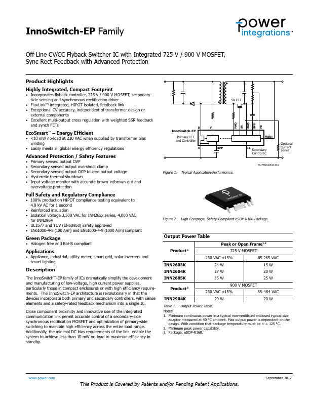
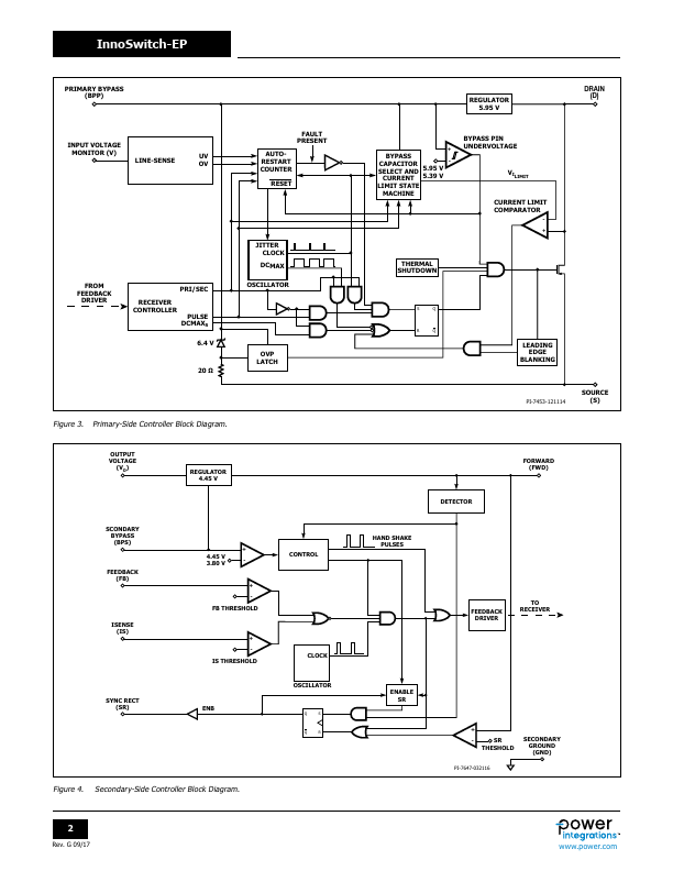
InnoSwitch-EP Family
Off-Line CV/CC Flyback Switcher IC with Integrated 725 V / 900 V MOSFET,
Sync-Rect Feedback with Advanced Protection
Product Highlights
Highly Integrated, Compact Footprint
• Incorporates flyback controller, 725 V / 900 V MOSFET, secondary-
side sensing and synchronous rectification driver
• FluxLink™ integrated, HIPOT-isolated, feedback link
• Exceptional CV accuracy, independent of transformer design or
external components
• Excellent multi-output cross regulation with weighted SSR feedback
and synch FETs
EcoSmart™ – Energy Efficient
• <10 mW no-load at 230 VAC when supplied by transformer bias
winding
• Easily meets all global energy efficiency regulations
Advanced Protection / Safety Features
• Primary sensed output OVP
• Secondary sensed output overshoot clamp
• Secondary sensed output OCP to zero output voltage
• Hysteretic thermal shutdown
• Input voltage monitor with accurate brown-in/brown-out and
overvoltage protection
Full Safety and Regulatory Compliance
• 100% production HIPOT compliance testing equivalent to
4.8 kV AC for 1 second
• Reinforced insulation
• Isolation voltage 3,500 VAC for INN26xx series, 4,000 VAC
for INN2904
• UL1577 and TUV (EN60950) safety approved
• EN61000-4-8 (100 A/m) and EN61000-4-9 (1000 A/m) compliant
Green Package
• Halogen free and RoHS compliant
Applications
• Appliance, industrial, utility meter, smart grid, solar inverters and
smart lighting
Description
The InnoSwitch™-EP family of ICs dramatically simplify the development
and manufacturing of low-voltage, high current power supplies,
particularly those in compact enclosures or with high efficiency require-
ments. The InnoSwitch-EP architecture is revolutionary in that the
devices incorporate both primary and secondary controllers, with sense
elements and a safety-rated feedback mechanism into a single IC.
Close component proximity and innovative use of the integrated
communication link permit accurate control of a secondary-side
synchronous rectification MOSFET and optimization of primary-side
switching to maintain high efficiency across the entire load range.
Additionally, the minimal DC bias requirements of the link, enable the
system to achieve less than 10 mW no-load to maximize efficiency in
standby.
SR FET
D
InnoSwitch-EP
Primary FET
and Controller
S
V
BPP
Figure 1. Typical Application/Performance.
VOUT
IS
Secondary
Control IC
Optional
Current
Sense
PI-7690-0011216
Figure 2. High Creepage, Safety-Compliant eSOP-R16B Package.
Output Power Table
Product 3
Peak or Open Frame1,2
725 V MOSFET
230 VAC ±15%
85-265 VAC
INN2603K
INN2604K
INN2605K
24 W
27 W
35 W
15 W
20 W
25 W
Product 3
900 V MOSFET
230 VAC ±15%
85-484 VAC
INN2904K
29 W
20 W
Table 1. Output Power Table.
Notes:
1. Minimum continuous power in a typical non-ventilated enclosed typical size
adapter measured at 40 °C ambient. Max output power is dependent on the
design. With condition that package temperature must be < = 125 °C.
2. Minimum peak power capability.
3. Package: eSOP-R16B.
www.power.com
This Product is Covered by Patents and/or Pending Patent Applications.
September 2017