PSMN025-100D
PSMN025-100D is N-channel TrenchMOS transistor manufactured by Philips Semiconductors.
FEATURES
- ’Trench’ technology
- Very low on-state resistance
- Fast switching
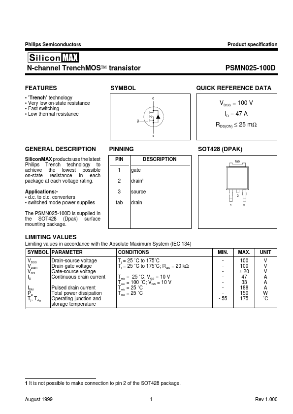
- Low thermal resistance g
QUICK REFERENCE DATA d
SYMBOL
VDSS = 100 V ID = 47 A RDS(ON) ≤ 25 mΩ s
GENERAL DESCRIPTION
Silicon MAX products use the latest Philips Trench technology to achieve the lowest possible on-state resistance in each package at each voltage rating. Applications:- d.c. to d.c. converters
- switched mode power supplies The PSMN025-100D is supplied in the SOT428 (Dpak) surface mounting package.
PINNING
PIN 1 2 3 tab gate drain1 source DESCRIPTION
SOT428 (DPAK) tab
2 drain
LIMITING VALUES
Limiting values in accordance with the Absolute Maximum System (IEC 134) SYMBOL PARAMETER VDSS VDGR VGS ID IDM PD Tj, Tstg Drain-source voltage Drain-gate voltage Gate-source voltage Continuous drain current Pulsed drain current Total power dissipation Operating junction and storage temperature CONDITIONS Tj = 25 ˚C to 175˚C Tj = 25 ˚C to 175˚C; RGS = 20 kΩ Tmb = 25 ˚C; VGS = 10 V Tmb = 100 ˚C; VGS = 10 V Tmb = 25 ˚C Tmb = 25 ˚C MIN.
- 55 MAX. 100 100 ± 20 47 33 188 150 175 UNIT V V V A A A W ˚C
1 It is not possible to make connection to pin 2 of the SOT428 package. August 1999 1 Rev 1.000
Philips Semiconductors
Product specification
N-channel Trench MOS™ transistor
AVALANCHE ENERGY LIMITING VALUES
Limiting values in accordance with the Absolute Maximum System (IEC 134) SYMBOL PARAMETER EAS Non-repetitive avalanche energy Non-repetitive avalanche current CONDITIONS Unclamped inductive load, IAS = 40 A; tp = 100 µs; Tj prior to avalanche = 25˚C; VDD ≤ 25 V; RGS = 50 Ω; VGS = 10 V; refer to fig:15
MIN.
- MAX. 260
UNIT m J
- 47
THERMAL RESISTANCES
SYMBOL PARAMETER Rth j-mb Rth j-a Thermal resistance junction to mounting base Thermal resistance junction to ambient CONDITIONS MIN. SOT428 package, pcb mounted, minimum footprint TYP. MAX. UNIT 50 1 K/W K/W
ELECTRICAL CHARACTERISTICS
Tj= 25˚C unless otherwise specified SYMBOL PARAMETER...