PL611S-19
PL611S-19 is PicoPLLTM KHz to MHz Programmable Clock manufactured by PhaseLink Corporation.
(Preliminary)
0.5k Hz-55MHz MHz to KHz Programmable Clock TM
Features
- Designed for Very Low-Power applications
- Offered in Tiny GREEN /Ro HS pliant packages o 6-pin DFN (2.0mmx1.3mmx0.6mm) o 6-pin SC70 (2.3mmx2.25mmx1.0mm) o 6-pin SOT23 (3.0mmx3.0mmx1.35mm)
- Input Frequency: o Reference Input: 1MHz to 200MHz o Non PLL mode, Ref input down to 10k Hz ..
- Accepts >0.1V reference signal input voltage
- Output frequency up to 55MHz CMOS. o <65MHz @ 1.8V operation o <90MHz @ 2.5V operation o <125MHz @ 3.3V operation
- One programmable I/O pin can be configured as Power Down (PDB) input, output Enable (OE), or Frequency Selection Switching input.
- Disabled outputs programmable as Hi Z or Active Low.
- Low current consumption: o <1.0m A with 27MHz & 32k Hz outputs o < 5µA when PDB is activated
- Single 1.8V, 2.5V, or 3.3V ± 10% power supply
- Operating temperature range from -40 ° C to 85 ° C
DESCRIPTION
The PL611s-19 is a low-cost general purpose frequency synthesizer and a member of Phase Link’s Factory Programmable ‘Quick Turn Clock (QTC)’ family. Phase Link’s PL611s-19 offers the versatility of using a single Reference Clock input and producing up to two (k Hz or MHz) system clock outputs. Designed for low-power applications with very stringent space requirement, PL611s-19 consumes <1.0m A, while producing 2 distinct outputs of 27MHz and 32k Hz. The power down feature of PL611s-19, when activated, allows the IC to consume less than 5µA of power. PL611s-19 fits in a small DFN, SC70, or SOT23 package. Cascading of the PL611s-19 with other Phase Link programmable clocks allow generating system level clocking requirements, thereby reducing the overall system implementation cost. In addition, one programmable I/O pin can be configured as Power Down (PDB) input, Output Enable (OE), or Frequency switching (FSEL). CLK1 can be programmed as (CLK0, FREF, FREF /2) output.
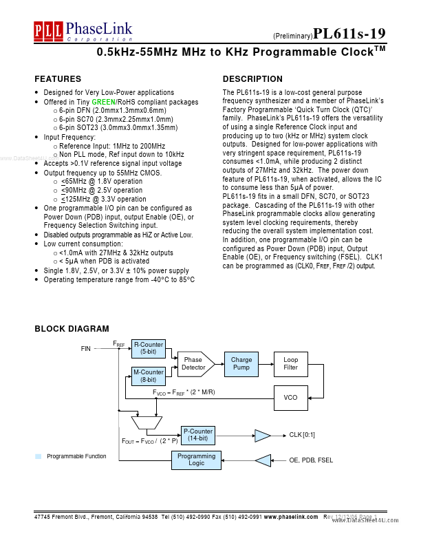
BLOCK DIAGRAM
FIN FREF R-Counter (5-bit) M-Counter (8-bit) Phase Detector Charge...