PLL650-07
FEATURES
- -
- -
- -
- - w w w
Full CMOS output swing with 40-m A output drive capability. 25-m A output drive at TTL level. Advanced, low power, sub-micron CMOS processes. 25MHz fundamental crystal or clock input. 2 outputs fixed at 50MHz, 2 outputs fixed at 25MHz . Zero PPM synthesis error in all clocks. Ideal for Network switches. 3.3V operation. Available in 14-Pin 150mil SOIC.
.D at h S a t e e
4U
. m o c
PRELIMINARY
LOW COST Network LAN Clock SOURCE
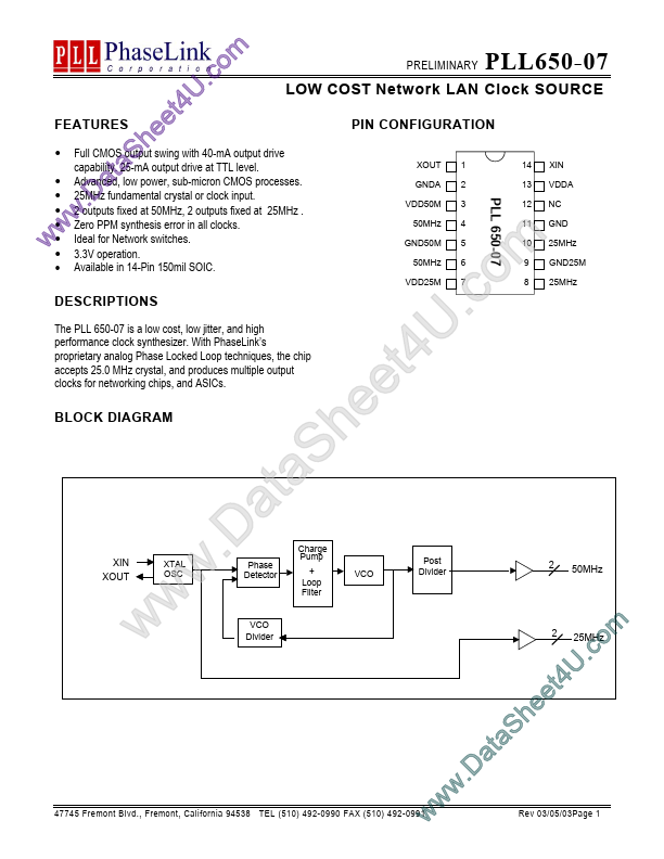
PIN CONFIGURATION
XOUT GNDA VDD50M 50MHz GND50M 50MHz VDD25M 1 2 14 13 XIN VDDA NC GND 25MHz GND25M 25MHz
PLL 650-07
3 4 5 6 7
12 11 10 9 8
DESCRIPTIONS
The PLL 650-07 is a low cost, low jitter, and high performance clock synthesizer. With Phase Link’s proprietary analog Phase Locked Loop techniques, the chip accepts 25.0 MHz crystal, and produces multiple output clocks for networking chips, and ASICs.
BLOCK DIAGRAM
XIN XOUT
XTAL OSC w w w
.D t a
S a
Charge Pump + Loop Filter e h
VCO t e
U 4
.c...