• Part: PI6C18551
  • Description: 3.3V/5V 1 to 4 Clock Buffer
  • Manufacturer: Pericom Semiconductor
  • Size: 294.47 KB
Download PI6C18551 Datasheet PDF
Pericom Semiconductor
PI6C18551
PI6C18551 is 3.3V/5V 1 to 4 Clock Buffer manufactured by Pericom Semiconductor.
Features - - - - - - - 160MHz maximum frequency Low skew: 250ps Fast rise/fall time: 1.5ns Output Enable with tri-states Industrial Temperature 3.3V or 5V power supply Packaging (Pb-free & Green available): - 8-pin SOIC (W) Description 
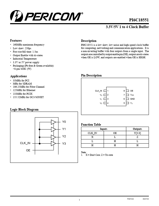
PI6C18551 is a low skew, low noise and high-speed clock buffer for puting, networking and munication applications. It is a non-inverting buffer with four outputs from a single input. The outputs are controlled by output enable pin (OE), outputs are tri-states when OE is LOW, and outputs are enabled when OE is HIGH. Applications - - - - - - 33MHz for PCI MHz for SDRAM 106.25MHz for Fibre Channel 125MHz for Ethernet 133MHz for PCIX 155.52MHz for OC3/SONET Pin Description CLK_IN Y0 Y1 Y2 1 2 3 4 8 7 6 5 OE VDD GND Y3 Logic Block Diagram Y0 Y1 Y2 CLK_IN OE Y3 Function Table Inputs CLK_IN X L H Note: 1. X = Don't Care; Z = Tri-state Outputs OE L H H Y[3:0] Z L H PS8733A 09/27/04 PI6C18551 3.3V/5V 1 to 4 Clock Buffer Pin Description Pin Name CLK_IN Y0 Y1 Y2 Y3 GND VDD OE Type Input Output Output Output Output Ground Power Input Pin No 1 2 3 4 5 6 7 8 Output clock Output clock Output clock Output clock GROUND 3.3V or 5V power supply Output Enable with pull-up resistor Descriptions Input clock with pull-up resistor External ponents A minimum number of external ponents are required for proper operation. A decoupling capacitor of 0.01μF should be connected between VDD on pin 7 and GND on pin 6, as close to the device as possible. A 33Ω series terminating resistor may be used on each clock output if the trace is longer than 1 inch. Absolute Maximun Ratings (Over operating free-air temperature range) Symbol VDD VI VO Ts Ta Tso Parameters Supply Voltage Input Voltage Output Voltage Storage Temperature Ambient Temperature Soldering Temperature -0.5 -0.5 -65 -40 Min. Max. 7 VDD+0.5 VDD+0.5 150 85 260 °C V Units PS8733A 09/27/04 PI6C18551 3.3V/5V 1 to 4 Clock Buffer DC Electrical Characteristics (VDD = 3.3V ±5%, TA = -40 to...