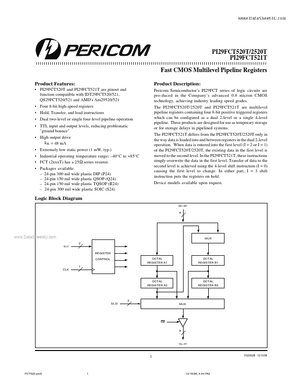
• Part: PI29FCT2520T
  • Description: FAST CMOS MULTILEVEL PIPELINE REGISTERS
  • Manufacturer: Pericom Semiconductor
  • Size: 85.51 KB
Download PI29FCT2520T Datasheet PDF
Pericom Semiconductor
PI29FCT2520T
PI29FCT2520T is FAST CMOS MULTILEVEL PIPELINE REGISTERS manufactured by Pericom Semiconductor.
Features : - PI29FCT520T and PI29FCT521T are pinout and function patible with IDT29FCT520/521, QS29FCT520/521 and AMD's Am29520/521 - Four 8-bit high-speed registers - Hold, Transfer, and load instructions - Dual two-level or single four-level pipeline operation - TTL input and output levels, reducing problematic "ground bounce" - High output drive IOL = 48 m A - Extremely low static power (1 m W, typ.) - Industrial operating temperature range: - 40°C to +85°C - FCT (2xxx T) has a 25 Ω series resistor. - Packages available: - 24-pin 300 mil wide plastic DIP (P24) - 24-pin 150 mil wide plastic QSOP (Q24) - 24-pin 150 mil wide plastic TQSOP (R24) - 24-pin 300 mil wide plastic SOIC (S24) Product Description : Peri Semiconductor’s PI29FCT series of logic circuits are pro-duced in the pany’s advanced 0.8 micron CMOS technology, achieving industry leading speed grades. The PI29FCT520T/2520T and PI29FCT521T are multilevel pipeline registers containing four 8-bit positive triggered registers which can be configured as a dual 2-level or a single 4-level pipeline. These products are designed for use as temporary storage or for storage delays in pipelined systems. The PI29FCT521T differs from the PI29FCT520T/2520T only in the way data is loaded into and between registers in the dual 2-level operation. When data is entered into the first level (I = 2 or I = 1) of the PI29FCT520T/2520T, the existing data in the first level is moved to the second level. In the PI29FCT521T, these instructions simply overwrite the data in the first level. Transfer of data to the second level is achieved using the 4-level shift instruction (I = 0) causing the first level to change. In either part, I = 3 shift instruction puts the registers on hold. Device models available upon request. Logic Block Diagram D0- D7 8 .. 2 I0,I1 REGISTER CONTROL 1 CLK OCTAL REGISTER A1 OCTAL REGISTER B1 OCTAL REGISTER A2 OCTAL REGISTER B2 S0,S1 2 MUX OE 8 Y0- Y7 PS2002B 12/10/96 FCT520.pm6 12/18/96,...