PI6LC48S25A
PI6LC48S25A is Ethernet Network Clock Generator manufactured by Pericom Semiconductor.
Features
ÎÎ3.3V & 2.5V supply voltage ÎÎCrystal/CMOS input: 25 MHz ÎÎDifferential input: 25MHz, 125MHz, and 156.25 MHz ÎÎOutput frequencies: 312.5, 156.25, 125, 100, 50, 25MHz ÎÎ4 Output banks with selectable output signaling: LVPECL or
LVDS ÎÎLow 0.3ps typical integrated phase noise design: 156.25MHz
(12k Hz to 20MHz) ÎÎPLL Bypass mode for test ÎÎPower supply noise rejection: -52 d Bc typical @ VDD ÎÎPackaging (Pb-free & Green): 56-lead 8×8mm TQFN ÎÎIndustrial temperature support: -40C to 85C
Description
The PI6LC48S25A is an LC VCO based low phase noise design intended for 10Gb E applications. Typical 10Gb E usage assumes a 25MHz crystal input, while the PLL loop is used to generate the 156.25MHz and other Ethernet clock frequencies. An additional buffered crystal oscillator output is provided to serve as a low noise reference for other circuitry. For Ethernet applications other than 10Gb E, programmable dividers allow for simultaneous output of 312.5, 156.25, 125, 100, 50, and 25MHz. This device offers both pin selection and I2C interface to give more options to meet various system needs.
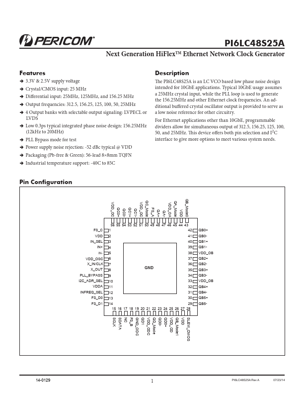
Pin Configuration
QB_Mode0 VDD
QA_Mode VDD_OA
QAQA+ FS_A QC_Mode VDD_OC QC1QC1+ QC0QC0+ VDD_OC
FS_C VDD IN_SEL
IN+
IN-
VDD_OSC X_IN/CLK
X_OUT PLL_BYPASS I2C_ADR_SEL
VDDA INFREQ_SEL
FS_D0 FS_D1
56 55 54 53 52 51 50 49 48 47 46 45 44 43
1 42
2 41
3 40
4 39
5 38
6 37
7 8 GND
36 35
9 34
10 33
11 32
12 31
13 30
14 29 15 16 17 18 19 20 21 22 23 24 25 26 27 28
QB0+ QB0QB1+ QB1VDD_OB QB2+ QB2QB3+ QB3VDD_OB QB4+ QB4QB5+ QB5-
SLEW_CMOS VDD QB_Mode1 VDD_OD QD0+ QD0QD_Mode VDD_ODC QD1 GND_ODC FS_B NC SDATA SCLK
14-0129
PI6LC48S25A Rev A
07/23/14
Block Diagram
Next Generation Hi Flex TM Ethernet Network Clock...