• Part: PI6C49X0210-A
  • Description: High Performance 1:10 Multi-Voltage CMOS Buffer
  • Manufacturer: Pericom Semiconductor
  • Size: 753.74 KB
Download PI6C49X0210-A Datasheet PDF
Pericom Semiconductor
PI6C49X0210-A
PI6C49X0210-A is High Performance 1:10 Multi-Voltage CMOS Buffer manufactured by Pericom Semiconductor.
Features - 10 single-ended outputs Fanout Buffer - Up to 200MHz output frequency - Ultra low output additive jitter = 0.05ps (typ.) - Selectable reference inputs support Xtal (10~50MHz), single- ended and differential - Low output skew ~ 50ps (typ.) - Propagation delay ~2ns (typ@3.3V) - 2.5V / 3.3V operation - User configurable output VDD in different banks: - Mixed 3.3V core/2.5V output operating supply - Mixed 3.3V core/1.8V output operating supply - Mixed 3.3V core/1.5V output operating supply - Mixed 2.5V core/1.8V output operating supply - Mixed 2.5V core/1.5V output operating supply - Industrial temperature range: - 40°C to +85°C - Packaging (Pb-free & Green available): - 32-pin TQFN (ZH) Applications - Networking systems including switches and Routers - High frequency backplane based puting and tele platforms Description 
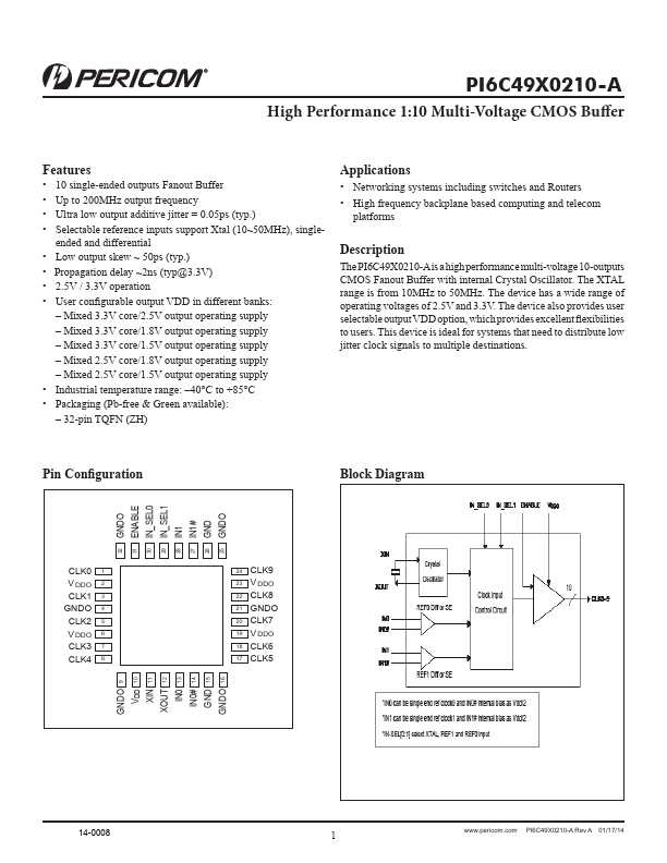
The PI6C49X0210-Ais a high performance multi-voltage 10-outputs CMOS Fanout Buffer with internal Crystal Oscillator. The XTAL range is from 10MHz to 50MHz. The device has a wide range of operating voltages of 2.5V and 3.3V. The device also provides user selectable output VDD option, which provides excellent flexibilities to users. This device is ideal for systems that need to distribute low jitter clock signals to multiple destinations. Pin Configuration Block Diagram GNDO ENABLE IN_SEL0 IN_SEL1 IN1 IN1# GND GNDO 32 31 30 29 28 27 26 25 CLK0 V DDO CLK1 GNDO CLK2 V DDO CLK3 CLK4 1 2 3 4 5 6 7 8 24 CLK9 23 V DDO 22 CLK8 21 GNDO 20 CLK7 19 V DDO 18 CLK6 17 CLK5 GNDO 9 VDD 10 XIN 11 XOUT 12 IN0 13 IN0# 14 GND 15 GNDO 16 14-0008 1 .peri. PI6C49X0210-A Rev A 01/17/14 High Performance 1:10 Multi-Voltage CMOS Buffer Pin Description Pin# Pin Name 1, 3, 5, 7, 8, 17, 18, 20, 22,...