Datasheet Summary
For munications Equipment
PLL LSI with Built-In Prescaler
Overview
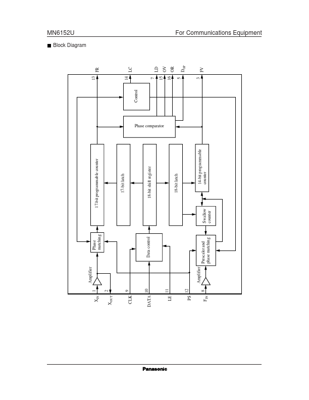
The MN6152U is a CMOS LSI for a phase-locked loop (PLL) frequency synthesizer with serial data input. It consists of a two-coefficient prescaler, variable frequency divider, phase parator, and charge pump. It offers high-speed operation on a low power supply voltage (1.8 to 2.5 V) and low power consumption (5 mW for VDD=2.0 V, F IN=100 MHz). Other Features include intermittent operation by the power save (PS) control signal and high-speed pull-in that rapidly corrects the phase differences occurring at the start of operation.
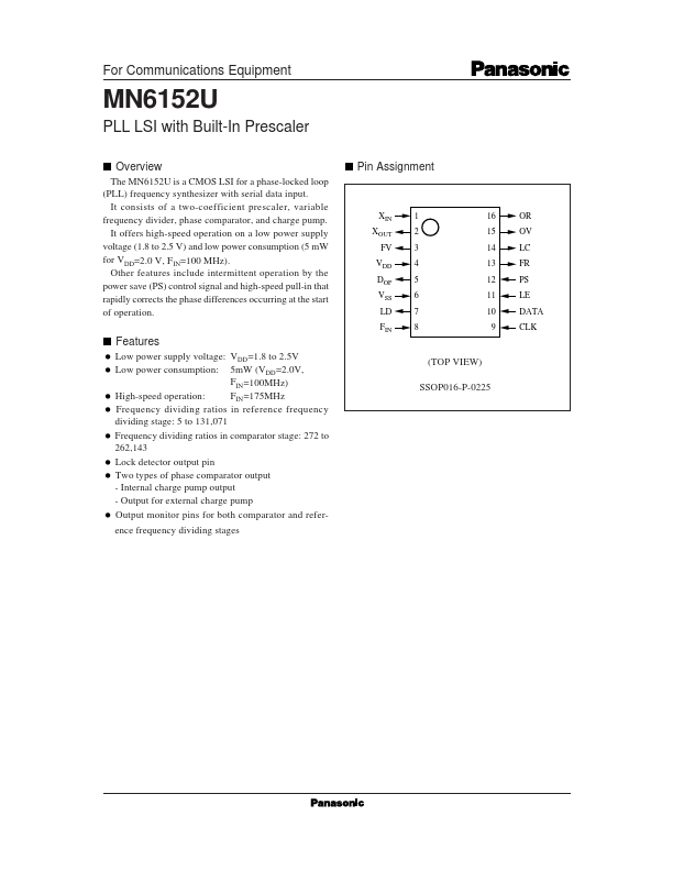
Pin Assignment
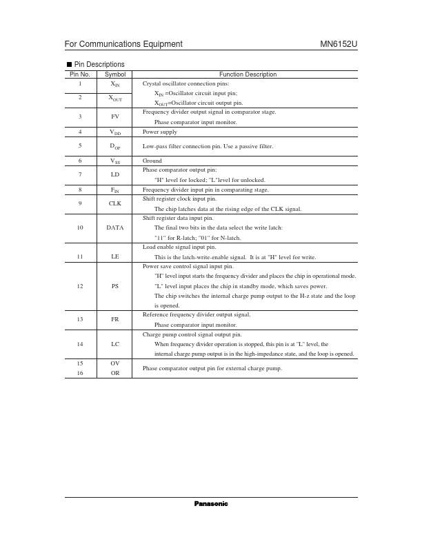
XIN XOUT FV VDD DOP VSS LD FIN
1 2 3 4 5 6 7 8
16 15 14 13 12 11...