2SC4026
Overview
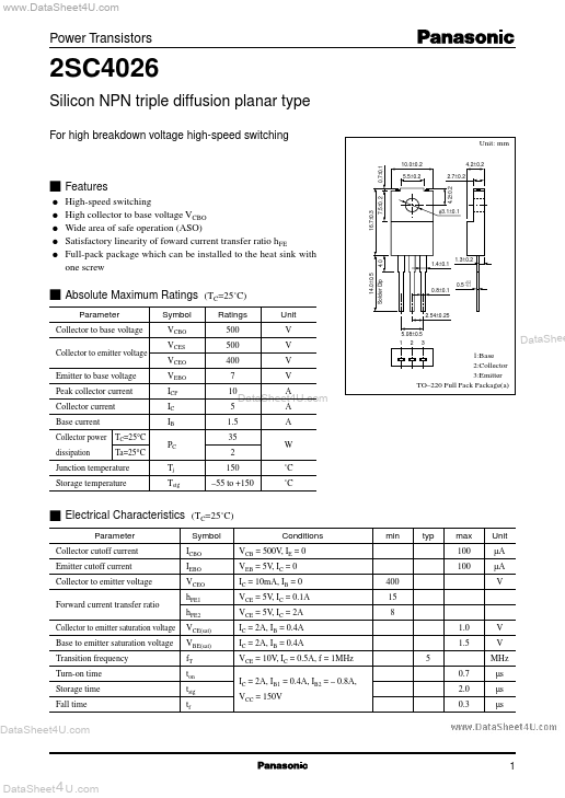
- 5±0.2
- 7±0.3 φ3.1±0.1
- 4±0.1
- 3±0.2
- 0±0.5 Solder Dip s Absolute Maximum Ratings Parameter Collector to base voltage Collector to emitter voltage Emitter to base voltage Peak collector current Collector current Base current Collector power TC=25°C dissipation Ta=25°C Junction temperature Storage temperature Symbol VCBO VCES VCEO VEBO ICP IC IB PC Tj Tstg
- 8±0.1
- 5 +0.2 -0.1
- 54±0.25 5.08±0.5 1 2 3 DataShee A A W ˚C ˚C A 1:Base 2:Collector 3:Emitter TO-220 Full Pack Package(a)
- 5 35 2 150 -55 to +150 s Electrical Characteristics Parameter Collector cutoff current Emitter cutoff current Collector to emitter voltage Forward current transfer ratio Collector to emitter saturation voltage Base to emitter saturation voltage Transition frequency Turn-on time Storage time Fall time (TC=25˚C) Symbol ICBO IEBO VCEO hFE1 hFE2 VCE(sat) VBE(sat) fT ton tstg tf Conditions VCB = 500V, IE = 0 VEB = 5V, IC = 0 IC = 10mA, IB = 0 VCE = 5V, IC = 0.1A VCE = 5V, IC = 2A IC = 2A, IB = 0.4A IC = 2A, IB = 0.4A VCE = 10V, IC = 0.5A, f = 1MHz IC = 2A, IB1 = 0.4A, IB2 = - 0.8A, VCC = 150V 5 0.7 2.0 0.3 400 15 8 1.0 1.5 V V MHz µs µs µs min typ max 100 100 Unit µA µA V 1 DataSheet 4 U .com Power Transistors PC - Ta