SN74LS299 Datasheet Text
SN74LS299
8- Bit Shift/Storage Register with 3- State Outputs
The SN74LS299 is an 8-Bit Universal Shift/Storage Register with
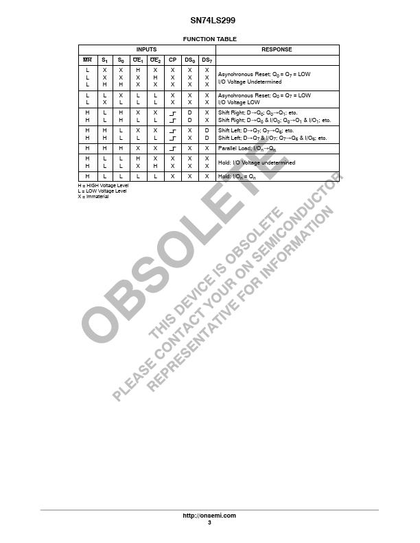
3-state outputs. Four modes of operation are possible: hold (store), shift left, shift right and load data.
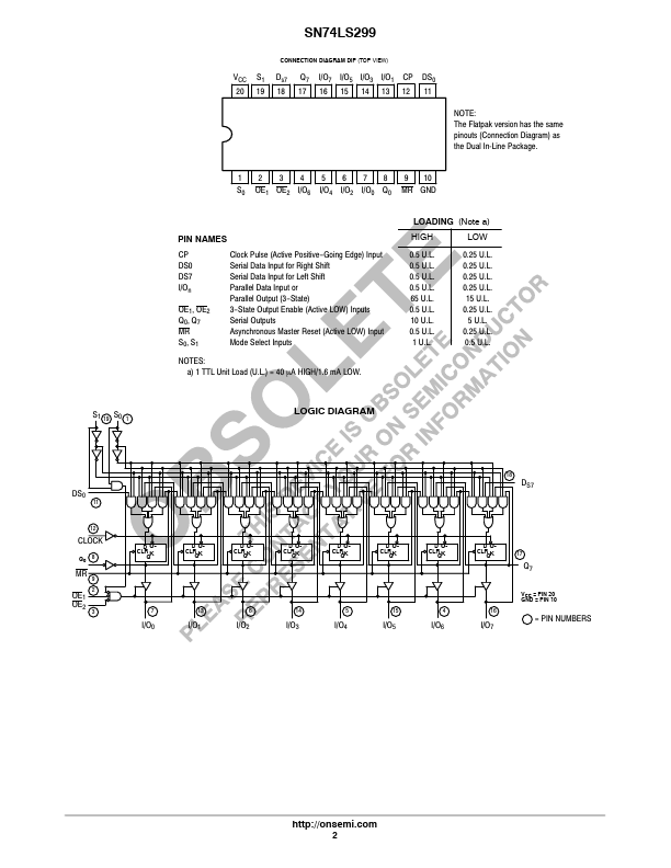
The parallel load inputs and flip-flop outputs are multiplexed to reduce the total number of package pins. Separate outputs are provided for flip-flops Q0 and Q7 to allow easy cascading. A separate active LOW Master Reset is used to reset the register.
- mon I/O for Reduced Pin Count
- Four Operation Modes: Shift Left, Shift Right, Load and Store
- Separate Shift Right Serial Input and Shift Left Serial Input for Easy
Cascading
- 3-State Outputs for Bus Oriented Applications
- Input Clamp Diodes Limit High-Speed Termination Effects
- ESD > 3500 Volts http://onsemi.
LOW POWER SCHOTTKY
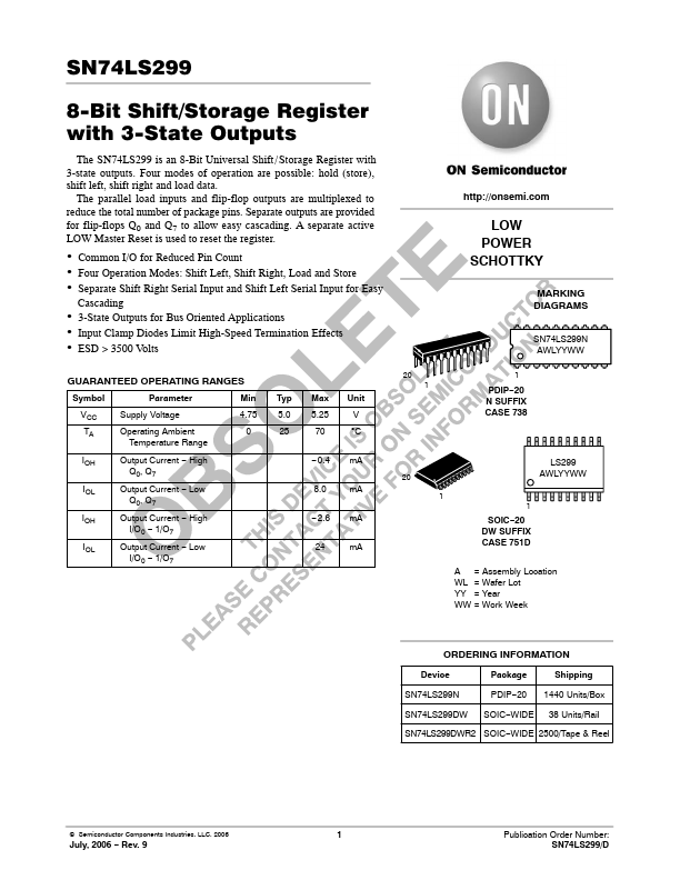
MARKING DIAGRAMS
SN74LS299N AWLYYWW
GUARANTEED OPERATING RANGES
Symbol
Parameter
Min Typ Max Unit
VCC
Supply Voltage
TA
Operating Ambient
Temperature Range
4.75 5.0 5.25
V
0
25
70
°C...