The following content is an automatically extracted verbatim text
from the original manufacturer datasheet and is provided for reference purposes only.
View original datasheet text
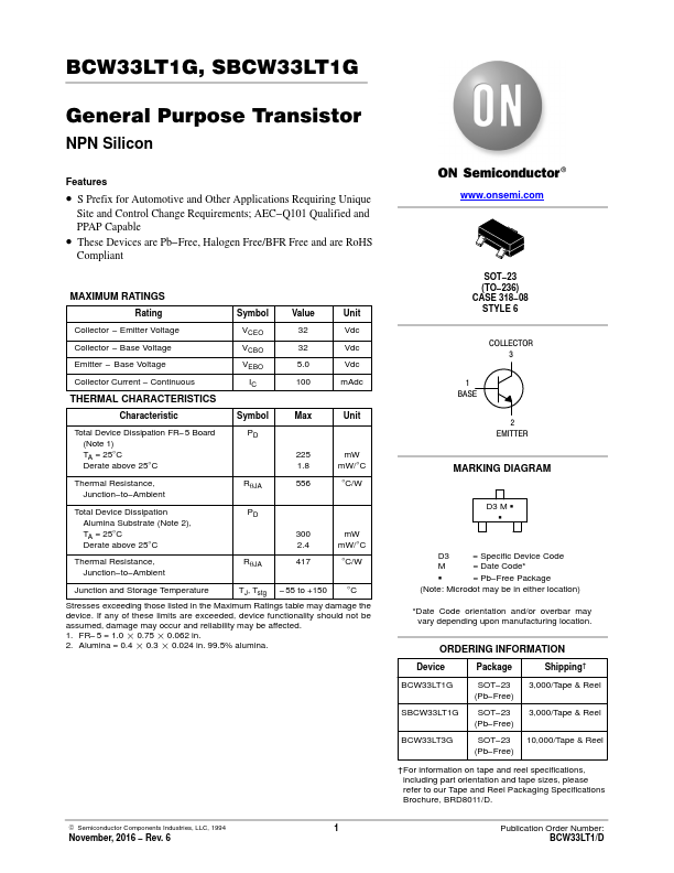
BCW33LT1G, SBCW33LT1G
General Purpose Transistor
NPN Silicon
Features
• S Prefix for Automotive and Other Applications Requiring Unique
Site and Control Change Requirements; AEC−Q101 Qualified and PPAP Capable
• These Devices are Pb−Free, Halogen Free/BFR Free and are RoHS
Compliant
MAXIMUM RATINGS
Rating
Symbol
Value
Unit
Collector − Emitter Voltage Collector − Base Voltage Emitter − Base Voltage Collector Current − Continuous THERMAL CHARACTERISTICS
VCEO VCBO VEBO
IC
32 Vdc 32 Vdc 5.0 Vdc 100 mAdc
Characteristic
Symbol
Max
Unit
Total Device Dissipation FR−5 Board
(Note 1)
TA = 25°C Derate above 25°C
PD
225 mW 1.8 mW/°C
Thermal Resistance, Junction−to−Ambient
RqJA
556 °C/W
Total Device Dissipation
Alumina Substrate (Note 2),
TA = 25°C Derate above 25°C
PD
300 mW 2.
 SBCW33LT1G Datasheet