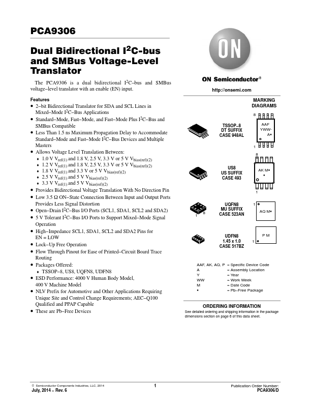
PCA9306
Function Description
The PCA9306 is a dual bidirectional I2C−bus and SMBus
voltage−level translator with an enable (EN) input, and is
operational from 1.0 V to 3.6 V (Vref(1)) and 1.8 V to 5.5 V
(Vbias(ref)(2)).
The PCA9306 allows bidirectional voltage translations
between 1.0 V and 5 V without the use of a direction pin. The
low ON−state resistance (Ron) of the switch allows
connections to be made with minimal propagation delay.
When EN is HIGH, the translator switch is on, and the SCL1
and SDA1 I/O are connected to the SCL2 and SDA2 I/O,
respectively, allowing bidirectional data flow between
ports. When EN is LOW, the translator switch is off, and a
high−impedance state exists between ports.
The PCA9306 is not a bus buffer that provides both level
translation and physical capacitance isolation to either side
of the bus when both sides are connected. The PCA9306
only isolates both sides when the device is disabled and
provides voltage level translation when active.
The PCA9306 can be used to run two buses, one at
400 kHz operating frequency and the other at 100 kHz
operating frequency. If the two buses are operating at
different frequencies, the 100 kHz bus must be isolated
when the 400 kHz operation of the other bus is required. If
the master is running at 400 kHz, the maximum system
operating frequency may be less than 400 kHz because of
the delays added by the translator.
As with the standard I2C−bus system, pull−up resistors are
required to provide the logic HIGH levels on the translator’s
bus. The PCA9306 has a standard open−collector
configuration of the I2C−bus. The size of these pull−up
resistors depends on the system, but each side of the
translator must have a pull−up resistor. The device is
designed to work with Standard−mode, Fast−mode and Fast
mode Plus I2C−bus devices in addition to SMBus devices.
The maximum frequency is dependent on the RC time
constant, but generally supports > 2 MHz.
When the SDA1 or SDA2 port is LOW, the clamp is in the
ON−state and a low resistance connection exists between the
SDA1 and SDA2 ports. Assuming the higher voltage is on
the SDA2 port, when the SDA2 port is HIGH, the voltage on
the SDA1 port is limited to the voltage set by VREF1. When
the SDA1 port is HIGH, the SDA2 port is pulled to the drain
pull−up supply voltage (Vpu(D)) by the pull−up resistors.
This functionality allows a seamless translation between
higher and lower voltages selected by the user without the
need for directional control. The SCL1/SCL2 channel also
functions as the SDA1/SDA2 channel.
All channels have the same electrical characteristics and
there is minimal deviation from one output to another in
voltage or propagation delay. This is a benefit over discrete
transistor voltage translation solutions, since the fabrication
of the switch is symmetrical. The translator provides
excellent ESD protection to lower voltage devices, and at the
same time protects less ESD−resistant devices.
FUNCTIONAL DIAGRAM
Figure 1. Logic Diagram
http://onsemi.com
2