P3P623S05A
Overview
- Clock distribution with Timing-Safe™ Peak EMI Reduction
- Input frequency range: 20MHz - 50MHz
- Multiple low skew Timing-safe™ Outputs: P3P623S05: 5 Outputs P3P623S09: 9 Outputs
- Supply Voltage: 3.3V±0.3V
- Packaging Information: P3P623S05: 8 pin TSSOP P3P623S09:16 pin TSSOP
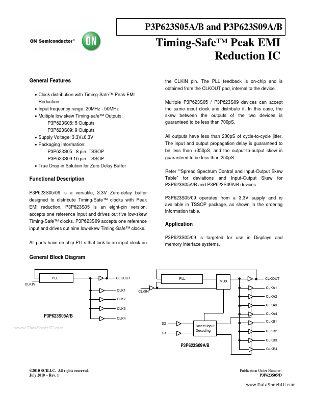
- True Drop-in Solution for Zero Delay Buffer All outputs have less than 200pS of cycle-to-cycle jitter. The input and output propagation delay is guaranteed to be less than ±350pS, and the output-to-output skew is guaranteed to be less than 250pS. Refer “Spread Spectrum Control and Input-Output Skew Table” for deviations and Input-Output Skew for P3P623S05A/B and P3P623S09A/B devices. P3P623S05/09 operates from a 3.3V supply and is available in TSSOP package, as shown in the ordering information table. Multiple P3P623S05 / P3P623S09 devices can accept the same input clock and distribute it. In this case, the skew between the outputs of the two devices is guaranteed to be less than 700pS. the CLKIN pin. The PLL feedback is on-chip and is obtained from the CLKOUT pad, internal to the device. Functional Description