Datasheet4U Logo Datasheet4U.com

P3P623S00E - Peak EMI Reduction IC

Datasheet Summary

Description

P3P623S00B/E is a versatile, 3.3 V Zero delay buffer designed to distribute Timing

Safe clocks with Peak EMI reduction.

pin version, accepts one reference input and drives out one low skew Timing

Safe clock.

Features

  • Clock Distribution with Timing.
  • Safe Peak EMI Reduction.
  • Input Frequency Range: 20 MHz.
  • 50 MHz.
  • 2 Different Spread Selection Options.
  • Spread Spectrum can be Turned ON/OFF.
  • External Input.
  • Output Delay Control Option.
  • Supply Voltage: 3.3 V ± 0.3 V.
  • P3P623S00B: 8 Pin SOIC P3P623S00E: 16 Pin TSSOP.
  • The First True Drop.
  • in Solution.
  • These Devices are Pb.
  • Free, Halogen Free/BFR Free.

📥 Download Datasheet

Datasheet preview – P3P623S00E

Datasheet Details

Part number P3P623S00E
Manufacturer ON Semiconductor
File Size 110.79 KB
Description Peak EMI Reduction IC
Datasheet download datasheet P3P623S00E Datasheet
Additional preview pages of the P3P623S00E datasheet.
Other Datasheets by ON Semiconductor

Full PDF Text Transcription

Click to expand full text
P3P623S00B, P3P623S00E Product Preview Timing-Safet Peak EMI Reduction IC Functional Description 
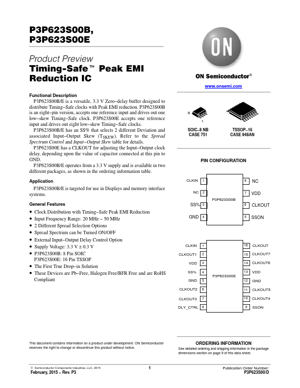
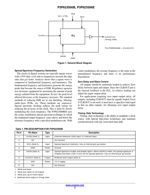
P3P623S00B/E is a versatile, 3.3 V Zero−delay buffer designed to distribute Timing−Safe clocks with Peak EMI reduction. P3P623S00B is an eight−pin version, accepts one reference input and drives out one low−skew Timing−Safe clock. P3P623S00E accepts one reference input and drives out eight low−skew Timing−Safe clocks. P3P623S00B/E has an SS% that selects 2 different Deviation and associated Input−Output Skew (TSKEW). Refer to the Spread Spectrum Control and Input−Output Skew table for details. P3P623S00E has a CLKOUT for adjusting the Input−Output clock delay, depending upon the value of capacitor connected at this pin to GND. P3P623S00B/E operates from a 3.
Published: |