The following content is an automatically extracted verbatim text
from the original manufacturer datasheet and is provided for reference purposes only.
View original datasheet text
P3P622S01J
Timing-Safet Peak EMI Reduction IC
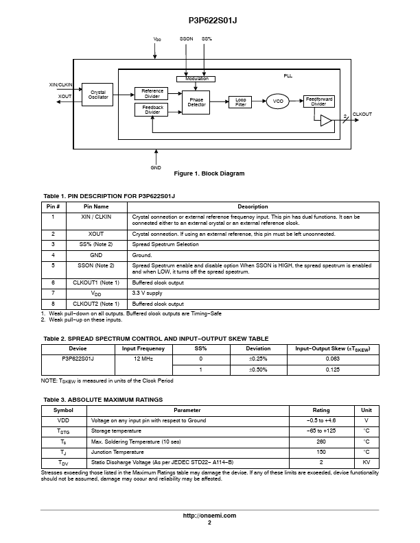
Functional Description P3P622S01J is a versatile, 3.3 V Zero−delay buffer designed to
distribute low frequency Timing−Safe Clocks with Peak EMI Reduction.
P3P622S01J accepts an input clock either from a fundamental Crystal or from an external reference clock.
P3P622S01J accepts one reference input and drives out two low−skew clocks.
P3P622S01J has an on−chip PLL that locks to an input reference clock. The PLL feedback is on−chip and is obtained from the CLKOUT pad, internal to the device.
Multiple P3P622S01J devices can accept the same input clock and distribute it. In this case, the skew between the outputs of the two devices is guaranteed to be less than 700 pS.
The output has less than 200 pS of cycle−to−cycle jitter.
 P3P622S01J Datasheet