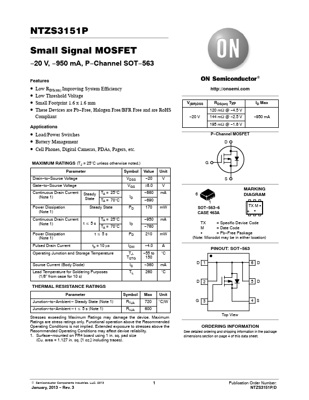
NTZS3151P
Features
- Low RDS(on) Improving System Efficiency
- Low Threshold Voltage
- Small Footprint 1.6 x 1.6 mm
- These Devices are Pb- Free, Halogen Free/BFR Free and are Ro HS pliant
Applications
- Load/Power Switches
- Battery Management
- Cell Phones, Digital Cameras, PDAs, Pagers, etc.
MAXIMUM RATINGS (TJ = 25°C unless otherwise noted.)
Parameter
Symbol Value
Drain- to- Source Voltage Gate- to- Source Voltage Continuous Drain Current
(Note 1)
Power Dissipation (Note 1)
Steady TA = 25°C State TA = 70°C
Steady State
VDSS VGS
- 20 ±8.0
- 860
- 690 170
Continuous Drain Current (Note 1)
Power Dissipation (Note 1) tv5s
TA = 25°C TA = 70°C tv5s
ID PD
- 950
- 760 210
Pulsed Drain Current tp = 10 ms
Operating Junction and Storage Temperature
Source Current (Body Diode) Lead Temperature for Soldering Purposes
(1/8″ from case for 10 s)
IDM TJ, TSTG IS TL
- 4.0
-...