Click to expand full text
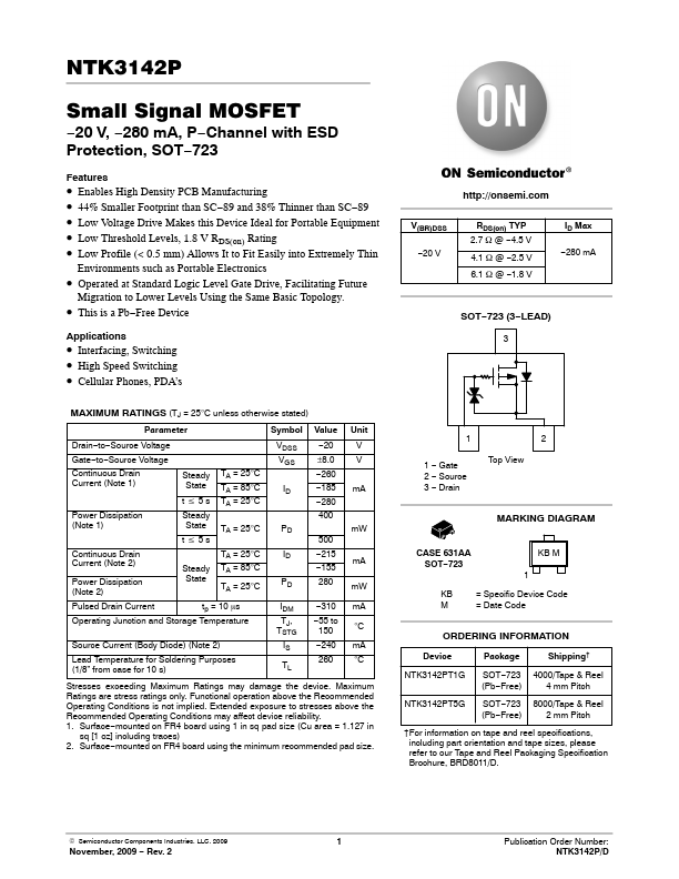
NTK3142P
Small Signal MOSFET
−20 V, −280 mA, P−Channel with ESD Protection, SOT−723
Features
• Enables High Density PCB Manufacturing • 44% Smaller Footprint than SC−89 and 38% Thinner than SC−89 • Low Voltage Drive Makes this Device Ideal for Portable Equipment • Low Threshold Levels, 1.8 V RDS(on) Rating • Low Profile (< 0.5 mm) Allows It to Fit Easily into Extremely Thin
Environments such as Portable Electronics
• Operated at Standard Logic Level Gate Drive, Facilitating Future
Migration to Lower Levels Using the Same Basic Topology.
• This is a Pb−Free Device
Applications
• Interfacing, Switching • High Speed Switching • Cellular Phones, PDA’s
http://onsemi.com
V(BR)DSS −20 V
RDS(on) TYP 2.7 W @ −4.5 V
4.1 W @ −2.5 V 6.1 W @ −1.
 NTK3142P Datasheet