Datasheet4U Logo Datasheet4U.com

NCV7519A - Hex Low-side MOSFET Pre-driver

Download the NCV7519A datasheet PDF. This datasheet also covers the NCV7519 variant, as both devices belong to the same hex low-side mosfet pre-driver family and are provided as variant models within a single manufacturer datasheet.
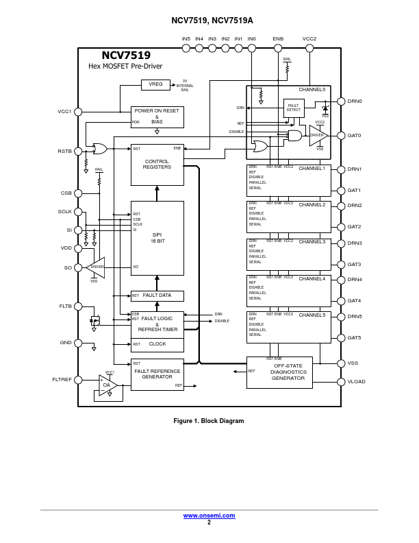
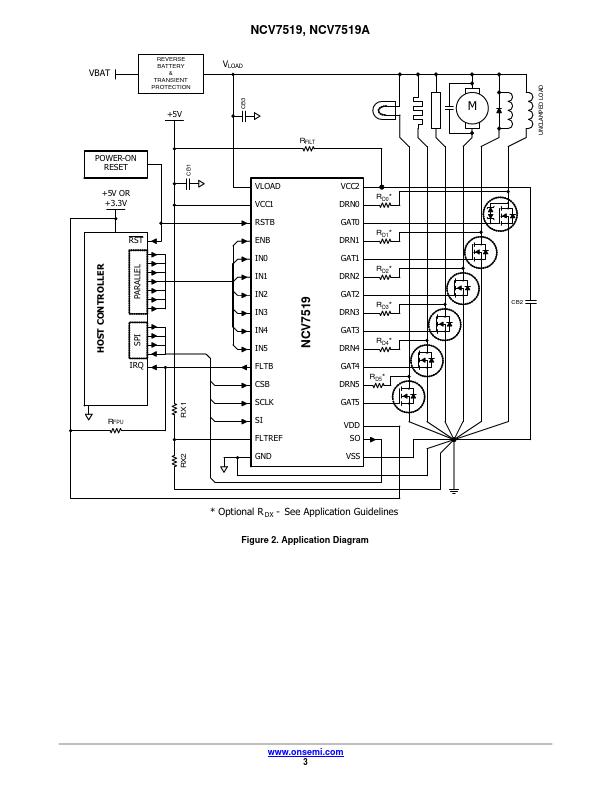
Description

32 PIN QFN EXPOSED PAD PACKAGE Label Description FLTREF Analog Fault Detect Threshold: 5 V Compliant DRN0 DRN5 Analog Drain Feedback GAT0 GAT5 Analog Gate Drive: 5 V Compliant RSTB Digital Master Reset Input: 3.3 V/5 V (TTL) Compatible ENB Digital Master Enable Input:

Features

  • 16.
  • bit SPI with Parity and Frame Error Detection.
  • 3.3 V/5 V Compatible Parallel and Serial Control Inputs.
  • 3.3 V/5 V Compatible Serial Output Driver.
  • Reset and Enable Inputs.
  • Open.
  • drain Fault Flag.
  • Priority Encoded Diagnostics with Latched Unique Fault Type Data.
  • Shorted Load, Short to GND.
  • Open Load.
  • On and Off State Pulsed Mode Diagnostics.
  • Ratiometric Diagnostic References and Currents.

📥 Download Datasheet

Note: The manufacturer provides a single datasheet file (NCV7519-ONSemiconductor.pdf) that lists specifications for multiple related part numbers.

Datasheet Details

Part number NCV7519A
Manufacturer onsemi
File Size 426.06 KB
Description Hex Low-side MOSFET Pre-driver
Datasheet download datasheet NCV7519A Datasheet

Full PDF Text Transcription (Reference)

The following content is an automatically extracted verbatim text from the original manufacturer datasheet and is provided for reference purposes only.

View original datasheet text
NCV7519, NCV7519A FLEXMOS] Hex Low-side MOSFET Pre-driver The NCV7519/A programmable six channel low−side MOSFET pre−driver is one of a family of FLEXMOS automotive grade products for driving logic−level MOSFETs. The product is controllable by a combination of serial SPI and parallel inputs. The device offers 3.3 V/ 5 V compatible inputs and the serial output driver can be powered from either 3.3 V or 5 V. An internal power−on reset provides controlled power up. A reset input allows external re−initialization and an enable input allows all outputs and diagnostics to be simultaneously disabled. Each channel independently monitors its external MOSFET’s drain voltage for fault conditions.
Published: |