Datasheet Details
| Part number | NCV57091C |
|---|---|
| Manufacturer | onsemi |
| File Size | 1.91 MB |
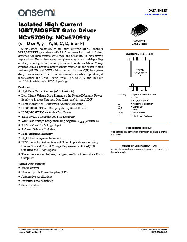
| Description | IGBT/MOSFET Gate Driver |
| Datasheet |
 NCV57091C Datasheet NCV57091C Datasheet
|
|
|
Download the NCV57091C datasheet PDF (NCV57090A included). The manufacturer datasheet provides complete specifications, pinout details, electrical characteristics, and typical applications for igbt/mosfet gate driver.
No.
Power Input side power supply.
and should be placed close to the pins for best results.
| Part number | NCV57091C |
|---|---|
| Manufacturer | onsemi |
| File Size | 1.91 MB |
| Description | IGBT/MOSFET Gate Driver |
| Datasheet |
NCV57091C Datasheet
|
|
|
|