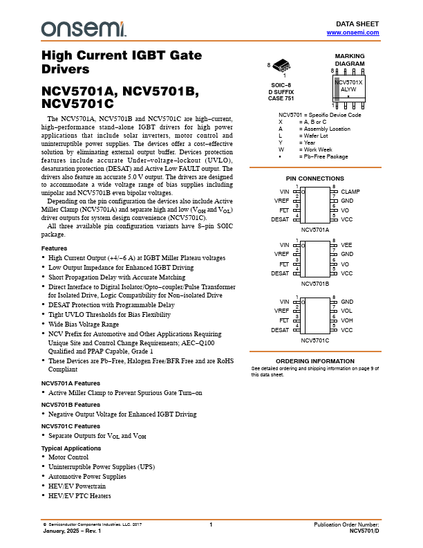
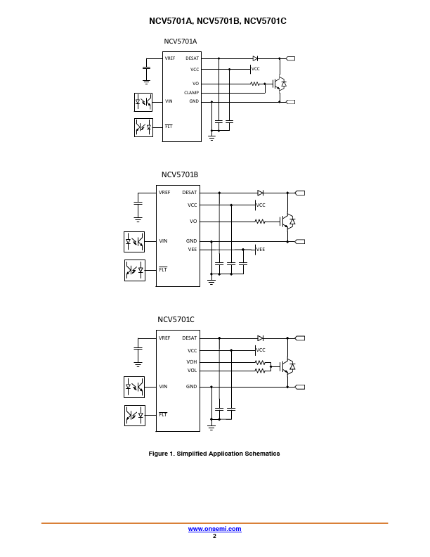
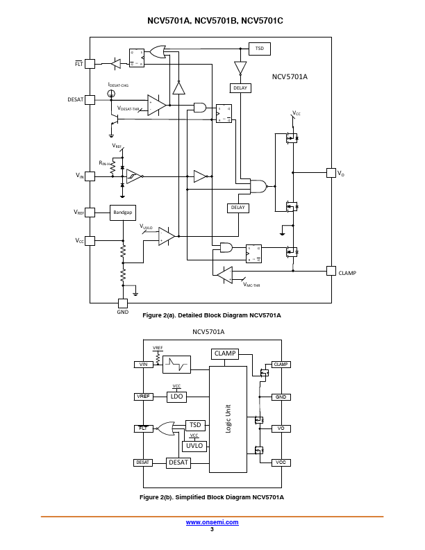
Datasheet Details
| Part number | NCV5701A |
|---|---|
| Manufacturer | onsemi |
| File Size | 541.31 KB |
| Description | High Current IGBT Gate Drivers |
| Datasheet |
 NCV5701A Datasheet NCV5701A Datasheet
|
|
|
No.
Input signal to control the output.
ed at the opto output, the pulse transformer secondary or the digital isolator output.
| Part number | NCV5701A |
|---|---|
| Manufacturer | onsemi |
| File Size | 541.31 KB |
| Description | High Current IGBT Gate Drivers |
| Datasheet |
NCV5701A Datasheet
|
|
|
|