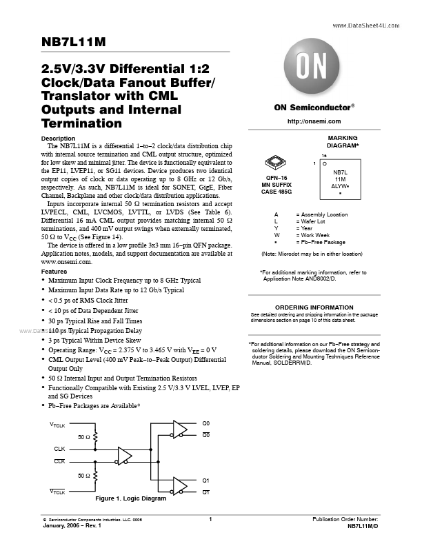
Datasheet4U Logo Datasheet4U.com

NB7L11M Datasheet

2.5v/3.3v Differential 1:2 Clock/data Fanout Buffer/ Translator

Manufacturer: onsemi

Datasheet Details

Part number NB7L11M
Manufacturer onsemi
File Size 240.17 KB
Description 2.5V/3.3V Differential 1:2 Clock/Data Fanout Buffer/ Translator
Datasheet NB7L11M_ONSemiconductor.pdf

NB7L11M Overview

MARKING DIAGRAM 16 1 The NB7L11M is a differential 1−to−2 clock/data distribution chip with internal source termination and CML output structure, optimized for low skew and minimal jitter. The device is functionally equivalent to the EP11, LVEP11, or SG11 devices. Device produces two identical output copies of clock or data operating up to 8 GHz or 12 Gb/s, respectively.

NB7L11M Key Features

  • Maximum Input Clock Frequency up to 8 GHz Typical
  • Maximum Input Data Rate up to 12 Gb/s Typical
  • < 0.5 ps of RMS Clock Jitter
  • < 10 ps of Data Dependent Jitter
  • 30 ps Typical Rise and Fall Times
  • 110 ps Typical Propagation Delay
  • 3 ps Typical Within Device Skew
  • Operating Range: VCC = 2.375 V to 3.465 V with VEE = 0 V
  • CML Output Level (400 mV Peak-to-Peak Output) Differential
  • ORDERING INFORMATION

NB7L11M Applications

  • Maximum Input Clock Frequency up to 8 GHz Typical
  • Maximum Input Data Rate up to 12 Gb/s Typical

NB7L11M Distributor