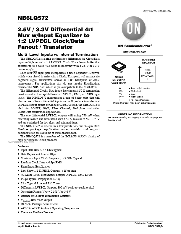
NB6LQ572 Overview
Key Specifications
Package: QFN
Mount Type: Surface Mount
Pins: 32
Operating Voltage: 2.5 V
Key Features
- 2 V and are optimized for low skew and minimal jitter. The NB6LQ572 is offered in a low profile 5x5 mm 32-pin QFN Pb -Free package. Application notes, models, and support documentation are available at . The NB6LQ572 is a member of the ECLinPS MAX™ family of high performance clock products
- Input Data Rate > 6.5 Gb/s Ty
