NB4N111K
NB4N111K is Clock Fanout Buffer manufactured by onsemi.
Description
The NB4N111K is a differential input clock 1 to 10 HCSL fanout buffer, optimized for ultra low propagation delay variation. The NB4N111K is designed with HCSL clock distribution for FBDIMM applications in mind. Inputs can accept differential VLPECL, CML, or VLDS levels.Single
- ended LVPECL, CML, VLCMOS or VLTTL levels are accepted with the proper VREFAC supply (see Figures 5, 10, 11, 12, and 13). Clock input pins incorporate an internal 50 W on die termination resistors. Outputs can interface with LVDS with proper termination (See Figure 15).
The NB4N111K specifically guarantees low output- to- output skews. Optimal design, layout, and processing minimize skew within a device and from device to device. System designers can take advantage of the NB4N111K’s performance to distribute low skew clocks across the backplane or the motherboard.
Features
- Typical Input Clock Frequencies: 100, 133, 166, 200, 266, 333, and
400 MHz
- 340 ps Typical Rise and Fall Times
- 800 ps Typical Propagation Delay
- Dtpd 100 ps Maximum Propagation Delay Variation Per Each
Differential Pair
- <1 ps RMS Additive Clock jitter
- Operating Range: VCC = 3.0 V to 3.6 V with VEE = 0 V
- Differential HCSL Output Level or LVDS with Proper Termination
- These are Pb- Free Devices http://onsemi.
1 32
QFN32 MN SUFFIX CASE 488AM
MARKING DIAGRAM-
32 1
NB4N 111K AWLYYWWG
= Assembly Site
WL = Wafer Lot
= Year
WW = Work Week
= Pb- Free Package
- For additional marking information, refer to Application Note AND8002/D.
VTCLK
CLK CLK
VTCLK VCC GND
Q0 Q0 Q1 Q1
Q8
Q8 Q9
RREF
IREF Q9
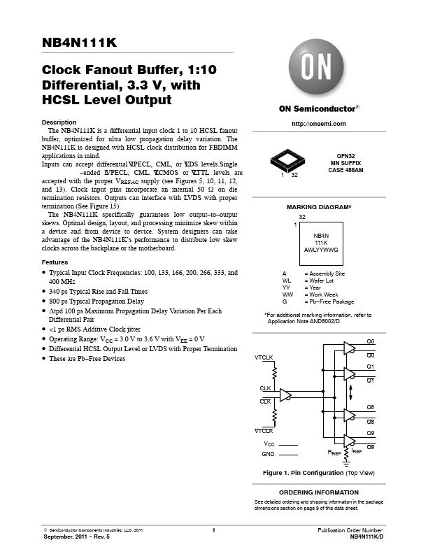
Figure 1. Pin Configuration (Top View)
ORDERING INFORMATION
See detailed ordering and shipping information in the package dimensions section on page 9 of this data...