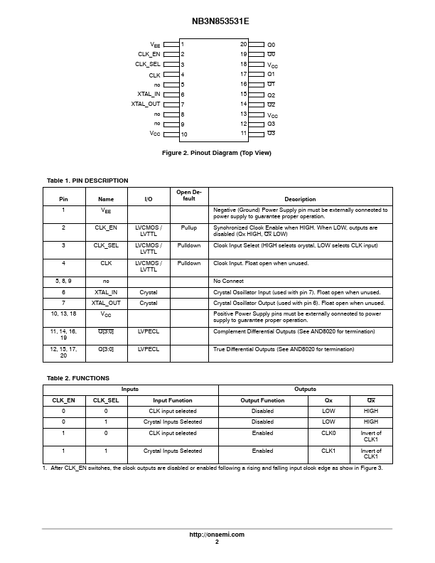
NB3N853531E Description
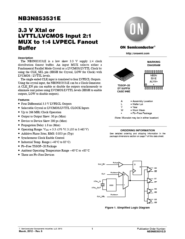
The NB3N853531E is a low skew 3.3 V supply 1:4 clock distribution fanout buffer. An input MUX selects either a Fundamental Parallel Mode Crystal or a LVCMOS/LVTTL Clock by using the CLK_SEL pin (HIGH for Crystal, LOW for Clock) with LVCMOS / LVTTL levels. The single ended CLK input is translated to four LVPECL Outputs.
NB3N853531E Key Features
- Four Differential 3.3 V LVPECL Outputs
- Selectable Crystal or LVCMOS/LVTTL CLOCK Inputs
- Up to 266 MHz Clock Operation
- Output to Output Skew: 30 ps (Max)
- Device to Device Skew 200 ps (Max)
- Propagation Delay 1.8 ns (Max)
- Operating Range: VCC = 3.3 ±5% V( 3.135 to 3.465 V)
- Additive Phase Jitter, RMS: 0.053 ps (Typ)
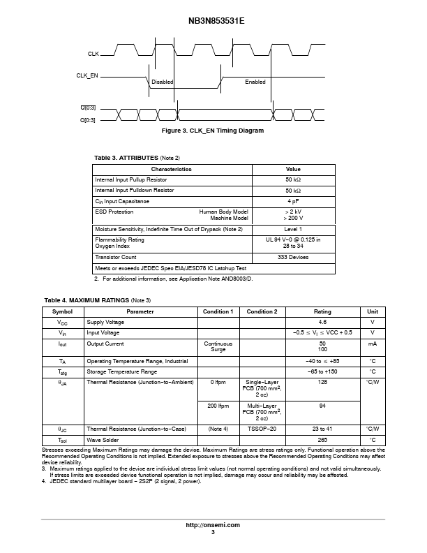
- Synchronous Clock Enable Control
- Industrial Temp. Range (-40°C to 85°C)