NB3N853501E Overview
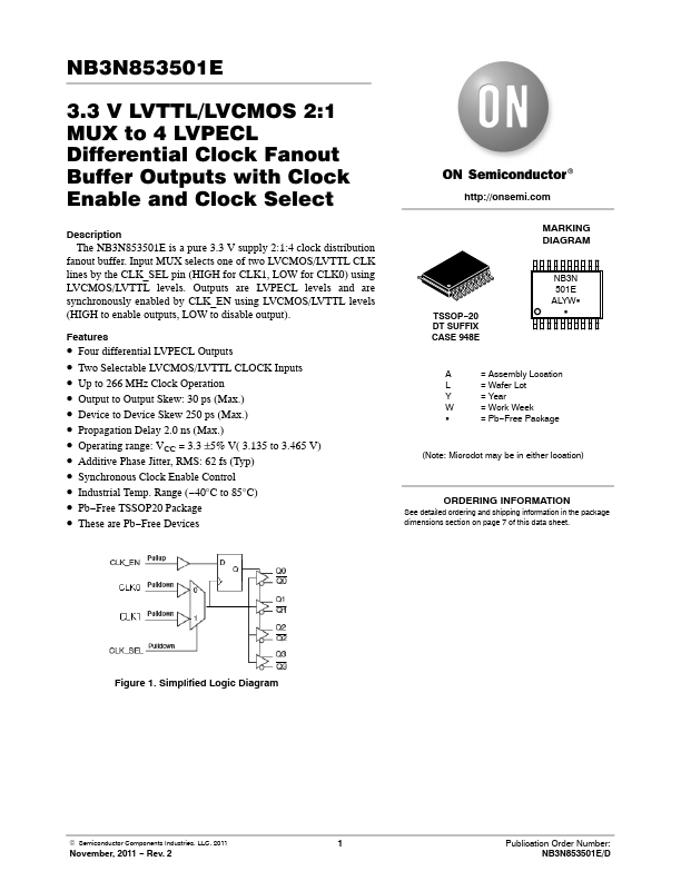
The NB3N853501E is a pure 3.3 V supply 2:1:4 clock distribution fanout buffer. Input MUX selects one of two LVCMOS/LVTTL CLK lines by the CLK_SEL pin (HIGH for CLK1, LOW for CLK0) using LVCMOS/LVTTL levels. Outputs are LVPECL levels and are synchronously enabled by CLK_EN using LVCMOS/LVTTL levels (HIGH to enable outputs, LOW to disable output).
NB3N853501E Key Features
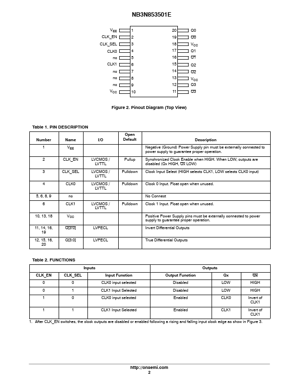
- Four differential LVPECL Outputs
- Two Selectable LVCMOS/LVTTL CLOCK Inputs
- Up to 266 MHz Clock Operation
- Output to Output Skew: 30 ps (Max.)
- Device to Device Skew 250 ps (Max.)
- Propagation Delay 2.0 ns (Max.)
- Operating range: VCC = 3.3 ±5% V( 3.135 to 3.465 V)
- Additive Phase Jitter, RMS: 62 fs (Typ)
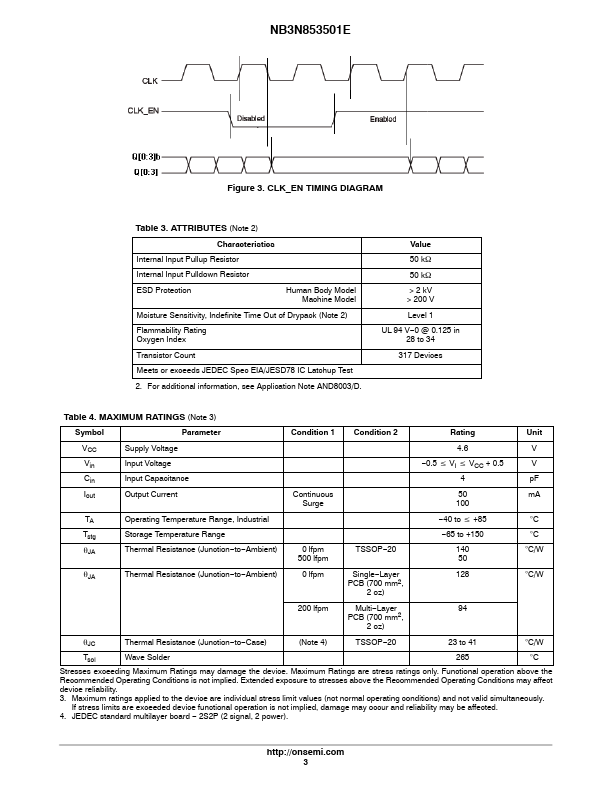
- Synchronous Clock Enable Control
- Industrial Temp. Range (-40°C to 85°C)