Datasheet4U Logo Datasheet4U.com

NB3N3020 - LVPECL/LVCMOS Clock Multiplier

Description

multiplier.

27 MHz fundamental mode parallel resonant crystal or a 2 210 MHz LVCMOS single ended clock source and generates a differential LVPECL output and a single ended LVCMOS/LVTTL output

Features

  • Selectable Clock Multiplier.
  • External Loop Filter is Not Required.
  • LVPECL Differential Output.
  • LVCMOS/ LVTTL Outputs.
  • RMS Period Jitter of 5 ps.
  • Jitter or Low Phase Noise at 125 MHz [25 MHz Input]: Offset Noise Power 100 Hz.
  • 95 dBc/Hz 1 kHz.
  • 107 dBc/Hz 10 kHz.
  • 112 dBc/Hz 100 kHz.
  • 117 dBc/Hz 1 MHz.
  • 117 dBc/Hz 10 MHz.
  • 134 dBc/Hz.
  • Operating Range 3.3 V ±10%.

📥 Download Datasheet

Datasheet Details

Part number NB3N3020
Manufacturer onsemi
File Size 131.48 KB
Description LVPECL/LVCMOS Clock Multiplier
Datasheet download datasheet NB3N3020 Datasheet
Other Datasheets by ON Semiconductor

Full PDF Text Transcription

Click to expand full text
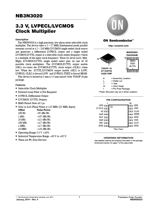
NB3N3020 3.3 V, LVPECL/LVCMOS Clock Multiplier 
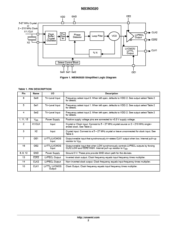
Description The NB3N3020 is a high precision, low phase noise selectable clock 
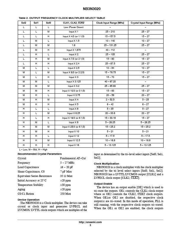
multiplier. The device takes a 5 – 27 MHz fundamental mode parallel resonant crystal or a 2 − 210 MHz LVCMOS single ended clock source and generates a differential LVPECL output and a single ended LVCMOS/LVTTL output at a selectable clock output frequency which is a multiple of the input clock frequency. Three tri−level (Low, Mid, High) LVCMOS/LVTTL single ended select pins set one of 26 possible clock multipliers. The LVCMOS/LVTTL output enable (OE1) tri−states the LVCMOS/LVTTL clock output (CLK1) when low. When the LVTTL/LVCMOS output enable (OE2) is LOW, LVPECL CLK2 is forced LOW and LVPECL CLK2 is forced HIGH. This device is housed in 5 mm x 4.
Published: |