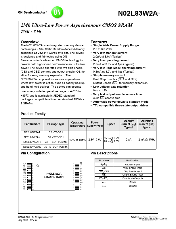
N02L83W2A Overview
CE1 H X L L L CE2 X L H H H WE X X L H H OE X X X2 L H I/O0 - I/O7 High Z High Z Data In Data Out High Z MODE Standby1 Standby Write2 Read Active 1 POWER Standby Standby Active Active Active 1. When the device is in standby mode, control inputs (WE and OE), address inputs and data input/outputs are internally isolated from any external influence and disabled from exerting any influence externally. When WE is...
N02L83W2A Key Features
- Single Wide Power Supply Range 2.3 to 3.6 Volts
- Very low standby current 2.0µA at 3.0V (Typical)
- Very low operating current 2.0mA at 3.0V and 1µs (Typical)
- Very low Page Mode operating current 0.8mA at 3.0V and 1µs (Typical)
- Simple memory control Dual Chip Enables (CE1 and CE2) Output Enable (OE) for memory expansion
- Low voltage data retention Vcc = 1.8V
- Very fast output enable access time 30ns OE access time
- Automatic power down to standby mode
- TTL patible three-state output driver
- TSOP I 32
N02L83W2A Applications
- Single Wide Power Supply Range 2.3 to 3.6 Volts