MC74VHCT32A Overview
Key Specifications
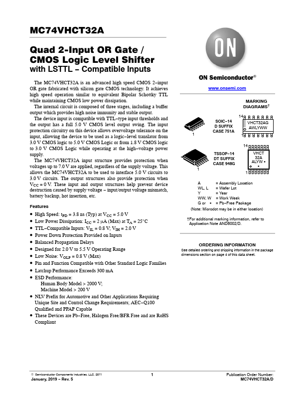
Package: TSSOP
Mount Type: Surface Mount
Pins: 14
Operating Voltage: 3.3 V
Key Features
- High Speed: tPD = 3.8 ns (Typ) at VCC = 5.0 V
- Low Power Dissipation: ICC = 2 mA (Max) at TA = 25°C
- TTL-Compatible Inputs: VIL = 0.8 V; VIH = 2.0 V
- Power Down Protection Provided on Inputs
- Balanced Propagation Delays