Datasheet4U Logo Datasheet4U.com

MC100EP195B - 3.3V ECL Programmable Delay Chip

Datasheet Summary

Description

designed primarily for clock deskewing and timing adjustment.

It provides variable delay of a differential NECL/PECL input transition.

Features

  • Maximum Input Clock Frequency >1.2 GHz Typical.
  • Programmable Range: 0 ns to 10 ns.
  • Delay Range: 2.2 ns to 12.2 ns.
  • 10 ps Increments.
  • PECL Mode Operating Range: VCC = 3.0 V to 3.6 V with VEE = 0 V.
  • NECL Mode Operating Range: VCC = 0 V with VEE =.
  • 3.0 V to.
  • 3.6 V.
  • IN/IN Inputs Accept LVPECL, LVNECL, LVDS Levels.
  • A Logic High on the EN Pin Will Force Q to Logic Low.
  • D[10:0] Can Select Either LVPECL, L.

📥 Download Datasheet

Datasheet preview – MC100EP195B

Datasheet Details

Part number MC100EP195B
Manufacturer ON Semiconductor
File Size 376.43 KB
Description 3.3V ECL Programmable Delay Chip
Datasheet download datasheet MC100EP195B Datasheet
Additional preview pages of the MC100EP195B datasheet.
Other Datasheets by ON Semiconductor

Full PDF Text Transcription

Click to expand full text
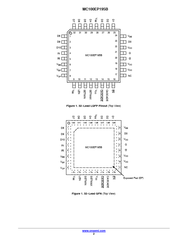
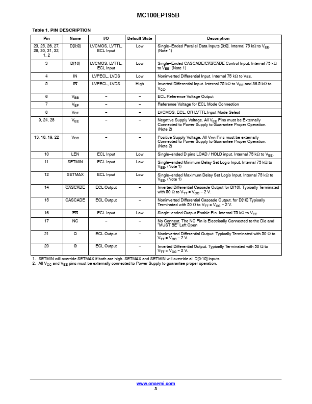
3.3 V ECL Programmable Delay Chip MC100EP195B Descriptions The MC100EP195B is a Programmable Delay Chip (PDC) designed primarily for clock deskewing and timing adjustment. It provides variable delay of a differential NECL/PECL input transition. The delay section consists of a programmable matrix of gates and multiplexers as shown in the logic diagram, Figure 2. The delay increment of the EP195B has a digitally selectable resolution of about 10 ps and a net range of up to 10.2 ns. The required delay is selected by the 10 data select inputs D[9:0] values and controlled by the LEN (pin 10). A LOW level on LEN allows a transparent LOAD mode of real time delay values by D[9:0]. A LOW to HIGH transition on LEN will LOCK and HOLD current values present against any subsequent changes in D[10:0].
Published: |