Datasheet Details
| Part number | FIN1019 |
|---|---|
| Manufacturer | onsemi |
| File Size | 1.99 MB |
| Description | 3.3V LVDS High Speed Differential Driver/Receiver |
| Datasheet |
 FIN1019 Datasheet FIN1019 Datasheet
|
|
|
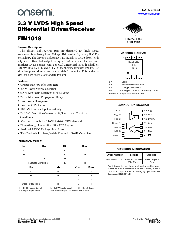
interconnects utilizing Low Voltage Differential Signaling (LVDS) technology.
| Part number | FIN1019 |
|---|---|
| Manufacturer | onsemi |
| File Size | 1.99 MB |
| Description | 3.3V LVDS High Speed Differential Driver/Receiver |
| Datasheet |
FIN1019 Datasheet
|
|
|
|
| Part Number | Description | Manufacturer |
|---|---|---|
| FIN1019 | 3.3V LVDS High Speed Differential Driver/Receiver | Fairchild Semiconductor |
| FIN1017 | 3.3V LVDS 1-Bit High Speed Differential Driver | Fairchild Semiconductor |
| FIN1018 | 3.3V LVDS 1-Bit High Speed Differential Receiver | Fairchild Semiconductor |
| FIN1001 | 3.3V LVDS 1-Bit High Speed Differential Driver | Fairchild Semiconductor |
| FIN1002 | LVDS 1-Bit High Speed Differential Receiver | Fairchild Semiconductor |
| Part Number | Description |
|---|---|
| FIN1001 | High-Speed Differential Driver |
| FIN1002 | High-Speed Differential Reciever |
The following content is an automatically extracted verbatim text from the original manufacturer datasheet and is provided for reference purposes only.