FDS8884
Overview
- Max rDS(on) = 23mΩ at VGS = 10V, ID = 8.5A
- Max rDS(on) = 30mΩ at VGS = 4.5V, ID = 7.5A
- Low gate charge
- 100% RG Tested
- RoHS Compliant *
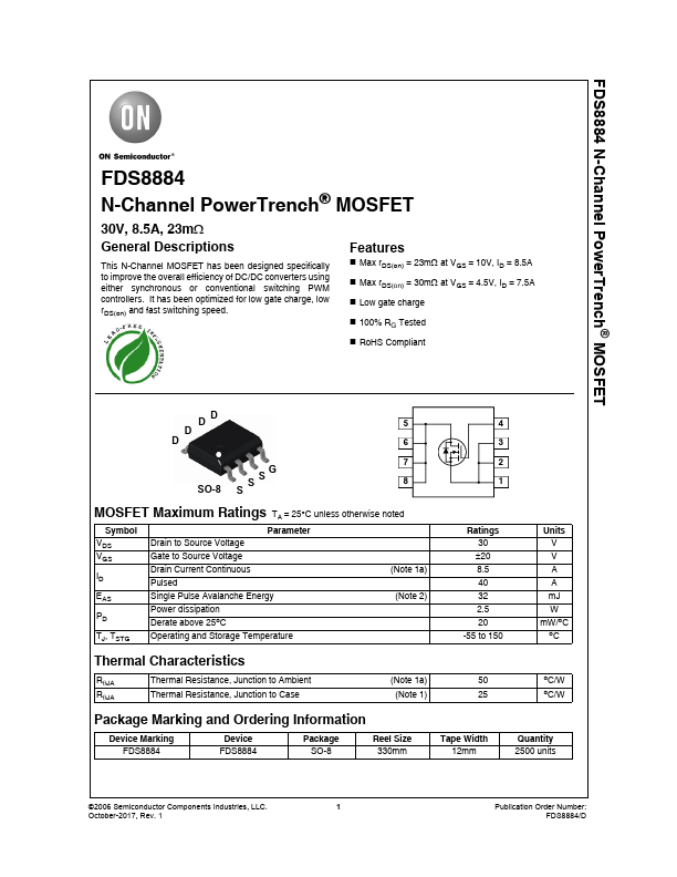
- 5 4 6 3 SO-8 G SS S 7 2 8 1 MOSFET Maximum Ratings TA = 25°C unless otherwise noted Symbol Parameter VDS Drain to Source Voltage VGS Gate to Source Voltage Drain Current Continuous ID Pulsed (Note 1a) EAS Single Pulse Avalanche Energy Power dissipation PD Derate above 25oC (Note 2)